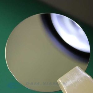
InPウェーハ
Indium phosphide (InP) is one of the important III-V compound semiconductors. It has the advantages of high electron mobility, good radiation resistance, and high band gap, which means that this material can amplify higher frequencies or signals with shorter wavelengths. Therefore, satellite receivers and amplifiers made of indium phosphide chips can work at extremely high frequencies above 100 GHz with high stability. Compared with gallium arsenide semiconductor materials, single crystal indium phosphide for sale from Ganwafer has a higher breakdown electric field and thermal conductivity, and higher electron mobility. More about our InP semiconductor wafer please see as follows:
- 説明
- 問い合わせ
説明
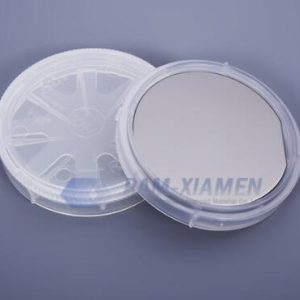
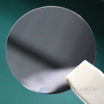
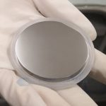
At present, the main sizes of InP single crystal substrates are 2-4 inches. From raw materials to ingots, indium phosphide is cut into a 2-inch or 4-inch wafer. The yield rate is generally about 28%, and the technical threshold is not generally high. The larger the indium phosphide wafer size, the higher the value.
1. Detail Specifications of Indium Phosphide Wafer
1.1. 4″ InP (Indium Phosphide) Single Crystal Wafer Specification
| アイテム | 仕様書 | |||
| ドーパント | N型 | N型 | P型 | SIタイプ |
| 伝導型 | 低ドープ | 硫黄 | 亜鉛 | lron |
| ウェーハの大口径 | 4 " | |||
| ウエハオリエンテーション | (100)が0.5°、±します | |||
| ウェーハ厚さ | 600±25um | |||
| プライマリフラット長 | 16±2mm | |||
| セカンダリフラット長 | 8±1mm | |||
| キャリア濃度 | ≤3x1016cm-3 | (0.8-6)x1018cm-3 | (0.6-6)x1018cm-3 | N / A |
| モビリティ | (3.5-4)x103cm2 / Vs | (1.5-3.5)x103cm2 / Vs | 50-70x103cm2 / Vs | > 1000cm2 / Vs |
| 抵抗率 | N / A | N / A | N / A | N / A |
| EPD | <1000cm-2 | <500cm-2 | <1x103cm-2 | <5x103cm-2 |
| TTV | <15um | |||
| 弓 | <15um | |||
| ワープ | <15um | |||
| レーザーマーキング | 要求に応じて | |||
| 表面仕上げ | P / E、P / P | |||
| エピ準備 | はい | |||
| パッケージ | シングルウェーハコンテナまたはカセット | |||
1.2. 3″ Indium Phosphide Wafer Substrate Specification
| アイテム | 仕様書 | |||
| ドーパント | N型 | N型 | P型 | SIタイプ |
| 伝導型 | 低ドープ | 硫黄 | 亜鉛 | lron |
| ウェーハの大口径 | 3 " | |||
| ウエハオリエンテーション | (100)が0.5°、±します | |||
| ウェーハ厚さ | 600±25um | |||
| プライマリフラット長 | 16±2mm | |||
| セカンダリフラット長 | 8±1mm | |||
| キャリア濃度 | ≤3x1016cm-3 | (0.8-6)x1018cm-3 | (0.6-6)x1018cm-3 | N / A |
| モビリティ | (3.5-4)x103cm2 / Vs | (1.5-3.5)x103cm2 / Vs | 50-70x103cm2 / Vs | > 1000cm2 / Vs |
| 抵抗率 | N / A | N / A | N / A | N / A |
| EPD | <1000cm-2 | <500cm-2 | <1x103cm-2 | <5x103cm-2 |
| TTV | <12um | |||
| 弓 | <12um | |||
| ワープ | <15um | |||
| レーザーマーキング | 要求に応じて | |||
| 表面仕上げ | P / E、P / P | |||
| エピ準備 | はい | |||
| パッケージ | シングルウェーハコンテナまたはカセット | |||
1.3。 2インチInPウェーハ基板仕様
| アイテム | 仕様書 | |||
| ドーパント | N型 | N型 | P型 | SIタイプ |
| 伝導型 | 低ドープ | 硫黄 | 亜鉛 | lron |
| ウェーハの大口径 | 2 " | |||
| ウエハオリエンテーション | (100)が0.5°、±します | |||
| ウェーハ厚さ | 350±25um | |||
| プライマリフラット長 | 16±2mm | |||
| セカンダリフラット長 | 8±1mm | |||
| キャリア濃度 | 3x1016cm-3 | (0.8-6)x1018cm-3 | (0.6-6)x1018cm-3 | N / A |
| モビリティ | (3.5-4)x103cm2 / Vs | (1.5-3.5)x103cm2 / Vs | 50-70x103cm2 / Vs | > 1000cm2 / Vs |
| 抵抗率 | N / A | N / A | N / A | N / A |
| EPD | <1000cm-2 | <500cm-2 | <1x103cm-2 | <5x103cm-2 |
| TTV | <10um | |||
| 弓 | <10um | |||
| ワープ | <12um | |||
| レーザーマーキング | 要求に応じて | |||
| 表面仕上げ | P / E、P / P | |||
| エピ準備 | はい | |||
| パッケージ | シングルウェーハコンテナまたはカセット | |||
2.リン化インジウムの分類と応用
導電性能に応じて、InP基板は主に半導電性基板と半絶縁性基板に分けられます。
半導体基板は、N型とP型の半導体基板に分類されます。 通常、In2S3とSnはN型基板のドーパントとして使用され、ZnP2はp型基板のドーパントとして使用されます。 さまざまなドーパントを使用する目的は、デバイス製造用にさまざまな導電率タイプの基板を提供することです。具体的には、次のとおりです。
※N型SドープInPは、レーザーダイオードだけでなく、光検出器にも使用されています。 転位による漏れ電流を回避するためには、Sをドープした転位のないリン化インジウム半導体が必要です。 硫黄はInP基板に明らかな不純物硬化効果があるため、転位のないリン化インジウムバルク単結晶は成長しやすいです。
※P型Znドープリン化インジウム(InP)は、主に高出力半導体レーザーに使用されています。 Znは不純物硬化効果も強いため、転位率を低くすることもできます。 レーザーの寿命を延ばすには、低転位が非常に重要です。
*半絶縁性InP基板は、ドープされているかどうかによって、ドープされた半絶縁性基板とドープされていない半絶縁性基板に分類されます。 ドープされた半絶縁性基板は通常、ドーパントとしてFe2Pを使用します。 ドープされていない半絶縁性基板は、高温アニーリングによる高純度のInP単結晶基板でできています。 半絶縁性リン化インジウム半導体基板は、主に無線周波数デバイスの製造に使用されます。