半導体チップの製造工程は、ウェーハ製造、ウェーハプローブ、パッケージング、初期試験、最終試験など、大きく分けて行うことができます。 なかでも、半導体ウェーハ製造工程とウェーハプローブ試験工程はフロントエンド半導体ウェーハ製造工程であり、組立工程と試験工程はバックエンド半導体製造工程である。
The main work of wafer manufacturing process from fab of Ganwafer is to make circuits and electronic components (such as transistors, capacitors, logic switches, etc.) on the wafer. The semiconductor manufacturing process steps are usually related to the product type and the semiconductor manufacturing technology used. Generally, the basic steps are to clean the wafer properly, then perform oxidation and chemical vapor deposition on its surface, and then perform repeated wafer making process such as coating, exposure, development, etching, ion implantation, and metal sputtering. Finally, several layers of circuits and components are processed and fabricated on the wafer.
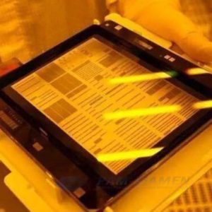
ウェーハプローブのテストプロセスは、前のプロセスの後にあります。 ウェーハ上に小さなグリッド、つまりダイが形成されます。 一般に、試験を容易にし、効率を改善するために、同じタイプのウェーハが同じウェーハ上に製造される。 ただし、必要に応じて品種や仕様の異なる製品を製造することもでき、各結晶粒をプローブ装置で検査することができます。
経験豊富で熟練した半導体ウェーハ製造会社として、私たちはクライアントの期待と要求を満たすためにこれらすべてのステップを正確に実行します。 予算内で業界標準の製品を製造・供給しています。