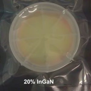
SiC / Si /サファイア基板上でのGaNエピタキシャル成長、サファイア/シリコン上のAlGaN、サファイア/シリコン上のAlN、サファイア上のInGaNを含むIII窒化物テンプレートは、研究者が2次元遷移金属ジスルフィドを成長させて電気的特性を測定するために提供できます。
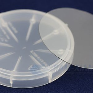
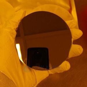
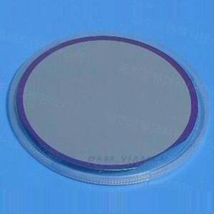
Group III nitride (including GaN, InGaN, AlN and its multi-element alloys) semiconductors are known as the third generation of semiconductor materials with wide band gap, high thermal conductivity, corrosion resistance and other excellent physical and chemical properties. So there are wide applications of GaN epi template in microelectronics and optoelectronics. However, due to the lack of homogeneous substrate materials, group III nitrides are generally grown on sapphire, SiC and Si substrates.
Ganwafer, a GaN epi wafer manufacturer, has adopted many methods to grow GaN epitaxy template. Generally, the GaN epi layer is prepared by epitaxial growth on the substrate material. Common GaN epitaxial growth methods include metal organic vapor phase epitaxy (MOCVD) and hydride vapor phase epitaxy method (HVPE), molecular beam epitaxy (MBE), and etc. The substrate material and the epitaxial layer constitute the GaN epiwafer template material. When Al and N elements are present in the epitaxial layer in the GaN epi process, the growth temperature of the epitaxial layer is very high, generally above 1200℃. This is due to the strong bond energy between Al atoms and N atoms. For the defect density of GaN epi growth, in order to meet the requirements of device preparation, the defect density in III nitrides is generally required to be less than 109cm-2.