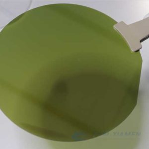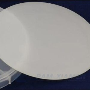
シリコンHEMTウェーハ上のGaN
Ganwafer offers GaN (Gallium Nitride) on Silicon (Si) Epitaxy HEMT wafer and GaN template on Si substrate. According to different applications, GaN on Silicon HEMT wafer can be classified into GaN-on-Silicon wafer for D-mode, GaN on Silicon substrate for E-mode and GaN on Silicon wafer for RF application. GaN based power electronic devices are still very expensive compared with Si devices. One of the ways to solve the cost problem is to fabricate GaN based heterostructures by epitaxy on Si substrate, and then to fabricate GaN based devices by complementary metal oxide semiconductor (CMOS) technology, so that the cost performance of the devices is better than that of Si devices. However, it is much more difficult to grow GaN on Silicon substrates than on SiC and sapphire substrates. The lattice mismatch ratio of GaN (0001) and Silicon (111) is as high as 16.9%, and the thermal expansion coefficient mismatch (thermal mismatch) is as high as 56%. These are main epitaxial challenges of GaN on Silicon, which may be able to be solved by introducing a buffer layer to GaN on Silicon wafer substrate. As a leading GaN on Silicon HEMT wafer manufacturer, we continuously develop our existing GaN on Silicon technology to gain a better wafer to you. And now please see below GaN on Si wafer specification:
- 説明
- 問い合わせ
説明
1.シリコンHEMTウェーハ上のGaN、Dモード
1.1シリコン上のGaNHEMTウェーハの仕様、Dモード
| ウェーハサイズ | 2 "、4"、6 "、8" |
| AlGaN / GaN HEMT構造 | 1.2を参照してください。 |
| キャリア密度 | > 9E12平方センチメートル |
| ホール移動度 | / |
| シート抵抗率 | / |
| 5x5um2のAFMRMS(nm) | <0.25nm |
| ボウ(UM) | <= 30um |
| エッジ除外 | <5ミリメートル |
| SiNパッシベーション層 | 0〜5nmの |
| u-GaNキャップ層 | 2nmの |
| Al組成 | 20から30パーセント |
| AlGaNバリア層 | / |
| GaNチャネル | / |
| AlGaNバッファ | / |
| AlNの | / |
| 基板材料 | シリコン基板 |
| Siウエハの厚み(μm) | 675um(2 ")、1000um(4")、1300um(6 ")、1500um(8") |
1.2シリコン上のGaNHEMTウェーハの構造、Dモード

2.シリコンHEMTエピタキシー上のGaN、E-MODE
| ウェーハサイズ | 2 "、4"、6 "、8" |
| AlGaN / GaN HEMT構造 | 1.2を参照してください。 |
| 残留2DEG密度(Vgを0 V) | <1e18 / cm3 |
| 5x5um2のAFMRMS(nm) | <0.25nm |
| ボウ(UM) | <= 30um |
| エッジ除外 | <5ミリメートル |
| p型GaN | / |
| u-GaNキャップ層 | / |
| Al組成 | 20から30パーセント |
| AlGaNバリア層 | / |
| GaNチャネル | / |
| AlGaNバッファ | / |
| 基板材料 | シリコン基板 |
| Siウエハの厚み(μm) | 675um(2 ")、1000um(4")、1300um(6 ")、1500um(8") |
3.RFアプリケーション用シリコン上の窒化ガリウムHEMTウェーハ
| ウェーハサイズ | 2 "、4"、6 "、8" |
| AlGaN / GaN HEMT構造 | 1.2を参照してください。 |
| キャリア密度 | > 9E12平方センチメートル |
| ホール移動度 | / |
| シート抵抗率 | / |
| 5x5um2のAFMRMS(nm) | <0.25nm |
| ボウ(UM) | <= 30um |
| エッジ除外 | <5ミリメートル |
| SiNパッシベーション層 | 0〜5nmの |
| u-GaNキャップ層 | / |
| Al組成 | 20から30パーセント |
| AlGaNバリア層 | / |
| GaNチャネル | / |
| AlGaNバッファ | / |
| AlNの | / |
| 基板材料 | シリコン基板 |
| Si基板の抵抗率(Ωcm)の | > 3000 |
| Siウエハの厚み(μm) | 1000um(2 ")、1000um(4")、1300um(6 ")、1500um(8") |
述べる:
中国政府は、半導体チップの製造に使用されるガリウム材料(GaAs、GaN、Ga2O3、GaP、InGaAs、GaSbなど)およびゲルマニウム材料の輸出に対する新たな制限を発表しました。 2023 年 8 月 1 日以降、これらの材料の輸出は中国商務省から許可を取得した場合にのみ許可されます。 ご理解いただければ幸いです。