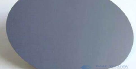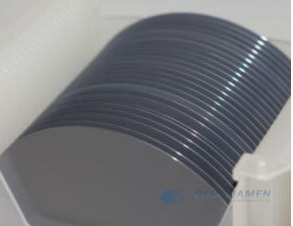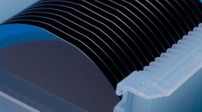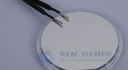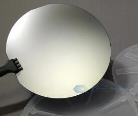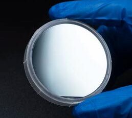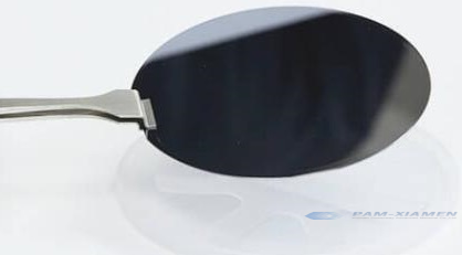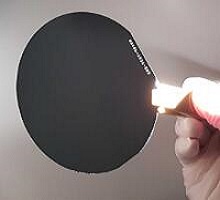
高純度アンドープ単結晶4H-SiCウェーハ
GaN / SiC HEMTマイクロ波デバイスは、新エネルギー車に適しています。 基板材料に関連する寄生容量によって引き起こされる信号損失を克服するために、絶縁性または半絶縁性基板を使用する必要があります。 したがって、半絶縁性SiC基板 is the preferred material for high-power GaN/SiC microwave HEMT devices. At present, most GaN/SiC HEMT devices are mostly vanadium-doped semi-insulating 4H-SiC wafer. The back-gate effect of vanadium-doped semi-insulating SiC substrates leads to the degradation of device performance or even failure, and vanadium will be produced in microwave devices. The back gate effect leads to defects such as current collapse, dispersion of leakage current at different frequencies and reduced output power. Therefore, the use of the intrinsic defects of SiC single crystals to introduce deep-level compensating shallow-level impurities to realize undoped high-purity semi-insulating 4H-SiC single crystal wafer has become a research hotspot in the field of silicon carbide. Ganwafer, one of a leading SiC wafer suppliers, can offer 4H silicon carbide (SiC) wafer as follows:
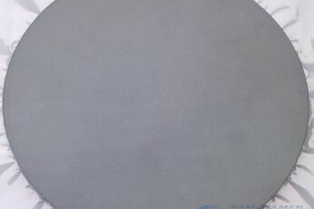
1. 4HSiCCVD単結晶ウェーハの仕様
4H undoped SiC CVD single crystal wafer GANW191204-SIC
* 633nmでの光吸収は、原材料の場合、1cmあたり0.1%未満です。
*または結晶成長のための>99.99%の高純度原料
SiCウェーハサイズ:外径2インチまたは50.8mm +/- 0.2mm
厚さ:0.33または0.35mmの厚さ
研究グレードまたは生産グレード
結晶方位:軸上[0001]+/-0.5度
一次フラット方向:軸上[1120]+/-5度
MPD:1cm2あたり15未満
両面研磨、Si面CMP、エピ対応
Si側粗さ0.5nm
反対側は1nmの粗さよりも優れています
TTV:10um
弓:<20um
ワープ<20um
2.4H-SiCウェーハの吸収率に関する研究
High purity optical crystals (from the visible range to the infrared rage up to Sum) are significant for potential applications, such as radiation-hardening, high operation temperature window and optoelectronic devices. For devices fabricated on SiC substrate, optical performance is very crucial subject. There are many researchers using infrared spectroscopy, which is a non-destructive, non-contact method, to study the optical properties of 4H silicon carbide. Ganwafer carried out researches on 4H SiC devices and found that the absorption rate of high purity undoped SiC substrate is >3%, more parameters please refer to the table below:
| Input power: 90mW, F500mm cylindrical lens | |||
| SiCの | 50.8mm | 中国から | |
| パスパワー | Feflパワー | 和 | 吸収 |
| 61.3 | 25.6 | 86.9 | 3.44% |
| 61.5 | 25.5 | 87 | 3.33% |
| 57 | 29.4 | 86.4 | 4.00% |
| 50.8 | 35.9 | 86.7 | 3.67% |
| 57.2 | 29.5 | 86.7 | 3.67% |
マーク:テストで使用された帯域は赤外線帯域(〜600-800nm)です。
詳細については、メールでお問い合わせください。sales@ganwafer.comとtech@ganwafer.com.