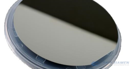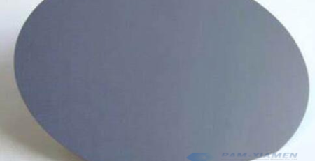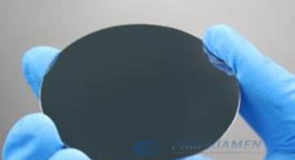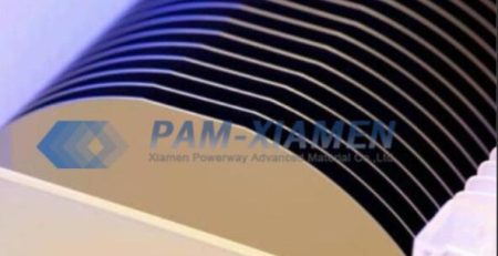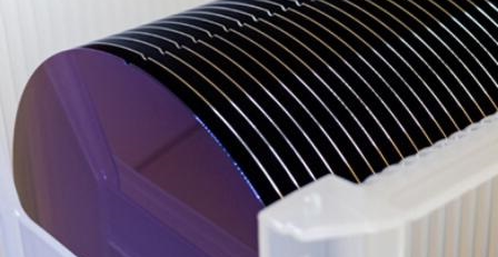
Wafer 4H-SiC a cristallo singolo non drogato ad alta purezza
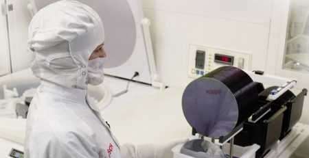
I dispositivi a microonde GaN/SiC HEMT sono adatti per veicoli a nuova energia. Per ovviare alla perdita di segnale causata dalla capacità parassita relativa al materiale del substrato, è necessario utilizzare un substrato isolante o semiisolante. Perciò,substrato semiisolante in SiC is the preferred material for high-power GaN/SiC microwave HEMT devices. At present, most GaN/SiC HEMT devices are mostly vanadium-doped semi-insulating 4H-SiC wafer. The back-gate effect of vanadium-doped semi-insulating SiC substrates leads to the degradation of device performance or even failure, and vanadium will be produced in microwave devices. The back gate effect leads to defects such as current collapse, dispersion of leakage current at different frequencies and reduced output power. Therefore, the use of the intrinsic defects of SiC single crystals to introduce deep-level compensating shallow-level impurities to realize undoped high-purity semi-insulating 4H-SiC single crystal wafer has become a research hotspot in the field of silicon carbide. Ganwafer, one of a leading SiC wafer suppliers, can offer 4H silicon carbide (SiC) wafer as follows:
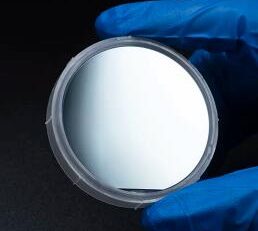
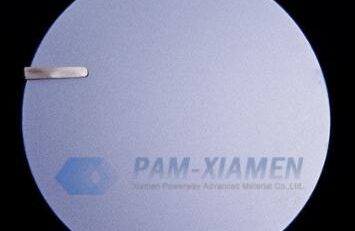
1. Specifiche del wafer a cristallo singolo 4H SiC CVD
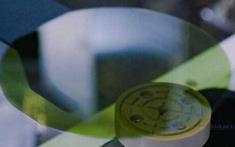
4H undoped SiC CVD single crystal wafer GANW191204-SIC
*Assorbimento ottico a 633 nm inferiore allo 0,1% per cm per la materia prima
* o materia prima di elevata purezza >99,99% per la crescita dei cristalli
Dimensioni wafer SiC: 2” OD o 50,8 mm +/-0,2 mm
Spessore: 0,33 o 0,35 mm di spessore
Grado di ricerca o grado di produzione
Orientamento del cristallo: sull'asse [0001] +/- 0,5 gradi
Orientamento piatto primario: sull'asse [1120] +/-5 gradi
MPD: meno di 15 per cm2
Lucidato su entrambi i lati, lato Si CMP, pronto per l'epi
Rugosità laterale Si 0,5 nm
L'altro lato è migliore della rugosità di 1 nm
TTV: 10um
Arco: <20um
Ordito <20um
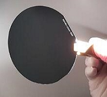
2. Studi sul tasso di assorbimento del wafer 4H-SiC
High purity optical crystals (from the visible range to the infrared rage up to Sum) are significant for potential applications, such as radiation-hardening, high operation temperature window and optoelectronic devices. For devices fabricated on SiC substrate, optical performance is very crucial subject. There are many researchers using infrared spectroscopy, which is a non-destructive, non-contact method, to study the optical properties of 4H silicon carbide. Ganwafer carried out researches on 4H SiC devices and found that the absorption rate of high purity undoped SiC substrate is >3%, more parameters please refer to the table below:
| Input power: 90mW, F500mm cylindrical lens | |||
| SiC | 50,8 mm | dalla Cina | |
| Passa il potere | Fefl potere | Somma | Assorbimento |
| 61.3 | 25.6 | 86.9 | 3,44% |
| 61.5 | 25.5 | 87 | 3,33% |
| 57 | 29.4 | 86.4 | 4,00% |
| 50.8 | 35.9 | 86.7 | 3,67% |
| 57.2 | 29.5 | 86.7 | 3,67% |
Mark: la banda utilizzata nel test è la banda degli infrarossi (~600-800 nm).
Per ulteriori informazioni, si prega di contattarci via e-mail all'indirizzosales@ganwafer.cometech@ganwafer.com.