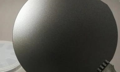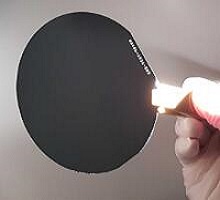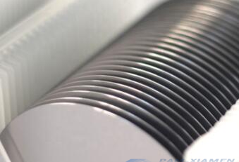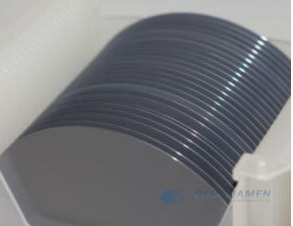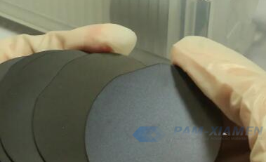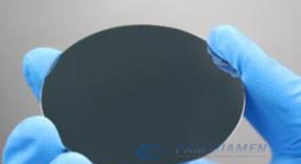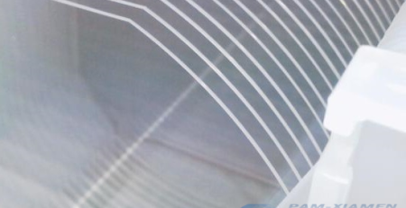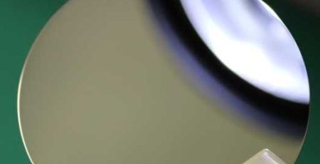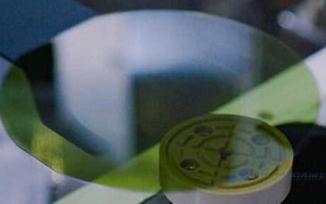
Hochreiner undotierter Einkristall-4H-SiC-Wafer
GaN/SiC-HEMT-Mikrowellengeräte eignen sich für neue Energiefahrzeuge. Um den Signalverlust zu überwinden, der durch parasitäre Kapazität in Bezug auf das Substratmaterial verursacht wird, muss ein isolierendes oder halbisolierendes Substrat verwendet werden. Deswegen,halbisolierendes SiC-Substrat is the preferred material for high-power GaN/SiC microwave HEMT devices. At present, most GaN/SiC HEMT devices are mostly vanadium-doped semi-insulating 4H-SiC wafer. The back-gate effect of vanadium-doped semi-insulating SiC substrates leads to the degradation of device performance or even failure, and vanadium will be produced in microwave devices. The back gate effect leads to defects such as current collapse, dispersion of leakage current at different frequencies and reduced output power. Therefore, the use of the intrinsic defects of SiC single crystals to introduce deep-level compensating shallow-level impurities to realize undoped high-purity semi-insulating 4H-SiC single crystal wafer has become a research hotspot in the field of silicon carbide. Ganwafer, one of a leading SiC wafer suppliers, can offer 4H silicon carbide (SiC) wafer as follows:
1. Spezifikationen für 4H-SiC-CVD-Einkristallwafer
4H undoped SiC CVD single crystal wafer GANW191204-SIC
*Optische Absorption bei 633 nm weniger als 0,1 % pro cm für Rohmaterial
* oder hochreines Rohmaterial >99,99 % für das Kristallwachstum
SiC-Wafergröße: 2 Zoll Außendurchmesser oder 50,8 mm +/-0,2 mm
Dicke: 0,33 oder 0,35 mm dick
Forschungsqualität oder Produktionsqualität
Kristallorientierung: auf Achse [0001] +/- 0,5 Grad
Primäre flache Ausrichtung: auf Achse [1120] +/-5 Grad
MPD: weniger als 15 pro cm2
Doppelseitig poliert, Si-Seite CMP, Epi-ready
Si-Seitenrauheit 0,5 nm
Andere Seite besser als 1nm Rauheit
TTV: 10um
Bogen: <20um
Warp <20um
2. Studien zur Absorptionsrate von 4H-SiC-Wafern
High purity optical crystals (from the visible range to the infrared rage up to Sum) are significant for potential applications, such as radiation-hardening, high operation temperature window and optoelectronic devices. For devices fabricated on SiC substrate, optical performance is very crucial subject. There are many researchers using infrared spectroscopy, which is a non-destructive, non-contact method, to study the optical properties of 4H silicon carbide. Ganwafer carried out researches on 4H SiC devices and found that the absorption rate of high purity undoped SiC substrate is >3%, more parameters please refer to the table below:
| Input power: 90mW, F500mm cylindrical lens | |||
| SiC | 50,8 mm | aus China | |
| Macht weitergeben | Fefl macht | Summe | Absorption |
| 61.3 | 25.6 | 86.9 | 3,44 % |
| 61.5 | 25.5 | 87 | 3,33 % |
| 57 | 29.4 | 86.4 | 4,00% |
| 50.8 | 35.9 | 86.7 | 3,67 % |
| 57.2 | 29.5 | 86.7 | 3,67 % |
Mark: Das im Test verwendete Band ist das Infrarotband (~600-800nm).
Für weitere Informationen kontaktieren Sie uns bitte per E-Mail untersales@ganwafer.comundtech@ganwafer.com.