GaN/Si HEMT Structure
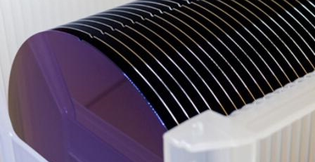
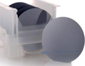
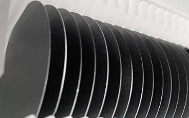
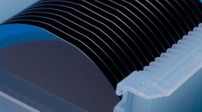
GaN has excellent physical properties such as high breakdown electric field strength and high thermal conductivity, making it an ideal material for fabricating high-frequency microwave devices and high-power power electronic devices. The quality of GaN epitaxial materials determines the performance of high electron mobility transistors (HEMTs). At present, the commonly used GaN HEMT device materials are prepared using heteroepitaxial methods. The most commonly used substrate materials for epitaxial GaN HEMT structure are silicon, sapphire, and SiC. Although there are significant thermal and lattice mismatches between silicon and GaN, we still use silicon based epitaxial GaN as the mainstream due to the mature process and low cost. Ganwafer provides GaN-on-Silicon HEMT wafers, taking the following specification as an example. Additional 2DEG GaN HEMT wafers, please visit https://www.ganwafer.com/product-category/gan-wafer/.
1. Si-based GaN HEMT Structure
GANW230414 – HEMT
| Epi layer | Material | Thickness | Doping |
| Top contact layer | GaN | – | 1e19cm-3 |
| Drift layer | GaN | – | – |
| Buried contact layer | GaN | 0.2 µm | – |
| Sub-drift layer | GaN | – | UID |
| Strain relief layers | – | – | – |
| Nucleation layer | AlN | – | – |
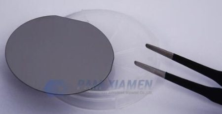
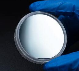
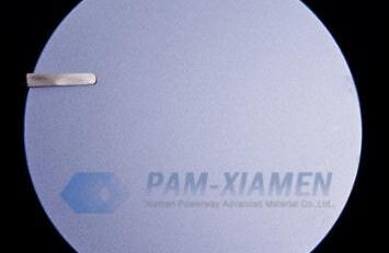
| Substrate | Si <111>, Dia. 150mm |
2. Influence of Substrate Deviation Angle on GaN Epitaxy
The surface morphology of GaN epitaxial layers grown on 4° and 2° off-axis Si substrates with orientation off angle for were studied, and analyzed the effect of off-angle on the surface morphology of GaN. The results showed that excessive substrate crystal orientation deviation angle can cause step like fluctuations on the surface of the epitaxial layer. However, for substrate crystal orientation deviation angle less than 2°, there are no steps on the surface, and the surface fluctuations are relatively smooth. Therefore, selecting a substrate with an off-angle within the range of 0.5-1° for GaN HEMT structure growth can reduce the roughness of the GaN epitaxial layers and the dislocations.
3. Effects of AlN Nucleation Layer for Si HEMT Structure with GaN Epilayer
There will be an influence of growth conditions of AlN layer on the crystal quality and stress state of GaN HEMT epitaxy. By adjusting the N/Al ratio, it was found that the smaller the N/Al ratio, the better the quality of GaN crystals and the smaller the stress state. By adjusting the TMAl flow rate and NH3 flow rate separately, it was found that the TMAl flow rate, rather than NH3 flow rate, affects the quality of GaN crystals. There is an optimal value for TMAl flow rate, at which the GaN crystal quality in GaN transistor structure is the best and the stress present in the epitaxial layer is the smallest.
Therefore, adjusting the TMAl flow rate mainly involves optimizing the growth rate of the AlN buffer layer, thereby optimizing the nucleation size during GaN 2DEG HEMT growth and reducing the occurrence of grain boundaries during merging, thus reducing the tensile stress in the GaN HEMT epitaxial layer.
For more information, please contact us email at sales@ganwafer.com and tech@ganwafer.com.