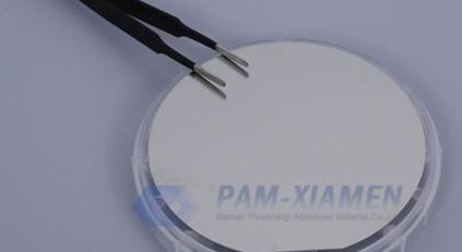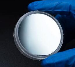
Structure de la diode électroluminescente GaInP / AlInP
Light emitting diode (LED) structure with GaInP / AlInP epilayers can be offered by Ganwafer. The ternary InGaP and AlInP materials are lattice matched to GaAs susbtrate, which can be grown by MOCVD. Growing high quality Matériau semi-conducteur ternaire III-V is important to the fabrication of light emitting diodes, laser diodes and multi-junction photovoltaic. Light emitting diode structure with ternary GaInP and AlInP epilayers from Ganwafer is shown as follows:
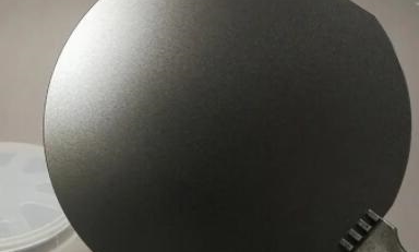
1. GaAs Epi Structure de la diode électroluminescente
No.1 GaAs LED Epitaxy
|
GaAs LED Structure (GANWP20065-LED) |
||
| Matériau de la couche | Épaisseur | Remarque |
| p-GaInP | - | Composition of In: 0.5;
mg dopée |
| p-GaP | - | |
| p-AlInP | - | |
| MQW | - | |
| n-AlInP | - | |
| DBR | - | |
| Arrêt de gravure n-GaInP | 20 nm | |
| Couche tampon | - | |
| sous-marins GaAs. | 350 um | |
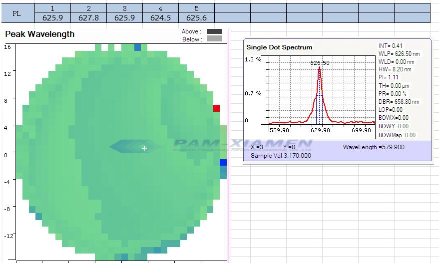
Le test PL et El de la tranche de diode électroluminescente quantique est illustré par le diagramme :
No. 2 GaAs based InGaP LED Epitaxy Wafer
GANW190724-INGAP
| Layer Name | Matériel | Épaisseur |
| P-cladding layer | P-AlInP | - |
| Active layer | MQW | - |
| N-cladding layer | N-AlInP | 900nm |
| Bragg reflector | N-AlGaAs/AlAs | - |
| Couche tampon | N-GaAs | |
| substrat | N-GaAs on-axis (100) plane without offcut |
No. 3 GaAs based LED Epitaxial Structure
GANWP19168-INGAP
| Layer Name | Matériel | Épaisseur |
| P-cladding layer | P-AlInP | - |
| Active layer | MQW | - |
| N-cladding layer | N-AlInP | - |
| Couche tampon | N-GaAs | 300nm |
| substrat | N-GaAs on-axis (100) plane without offcut |
2. FAQ of GaAs Light Emitting Diode Wafer
Q:We observed two MQW regions in GaInP LED wafer (GANWP19168-INGAP), illustrated in below figure. There are 9 pairs in each MQW separated by a thick barrier layer. May I know any reason to grow this kind of structure instead of a single stack of MQWs?
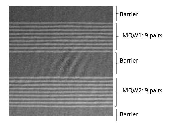
A: These are two groups of identical quantum wells in InGaP LED epitaxy. In order to increase the thickness of the active region and improve the reliability of the LED chip, the middle layer can be used normally without any influence on the photoelectric performance.
3. InGaP on GaAs for Light Emitting Diode Structure
InGaP, qui présente un grand potentiel pour remplacer les matériaux contenant de l'aluminium, est un matériau semi-conducteur critique généralement développé sur un substrat GaAs. Ses propriétés sont étroitement liées aux conditions de croissance, telles que la méthode de croissance, la température du substrat, le taux de croissance, l'orientation du substrat, le rapport III/V, etc. Ainsi, InGaP est idéal pour la croissance d'hétérostructures pour plusieurs applications, telles que les LED rouges à haute luminosité.
L'attractivité de l'hétérostructure InGaP / GaAs provient de son alignement de bande, le décalage de la bande de valence (AEv = 0,24 - 0,40 eV) est significativement plus grand que le décalage de la bande de conduction (Mc = 0,03 - 0,22 eV). Ceci est considéré comme plus favorable que la structure de bande du système hétéro AlGaAs / GaAs.
InGaP est une gravure hautement sélective sur GaAs, qui est utilisé comme couche d'arrêt de gravure dans notre structure épitaxiale de LED. Cela augmentera l'uniformité et la fabricabilité des dispositifs à microdiodes électroluminescentes. Mais la couche d'arrêt de gravure GaInP augmentera la hauteur de la barrière d'énergie qui doit être surmontée lorsque les électrons circulent du collecteur au sous-collecteur. Dans ces conditions, le gain de courant continu de la structure de LED MQW diminuera. Ainsi, la couche d'arrêt de gravure d'InGaP doit être suffisamment fine pour garantir les performances du dispositif.
Pour plus d'informations, veuillez nous contacter par e-mail à sales@ganwafer.com et tech@ganwafer.com.