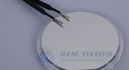
Struktura diody elektroluminescencyjnej GaInP / AlInP
Light emitting diode (LED) structure with GaInP / AlInP epilayers can be offered by Ganwafer. The ternary InGaP and AlInP materials are lattice matched to GaAs susbtrate, which can be grown by MOCVD. Growing high quality Trójskładnikowy materiał półprzewodnikowy III-V is important to the fabrication of light emitting diodes, laser diodes and multi-junction photovoltaic. Light emitting diode structure with ternary GaInP and AlInP epilayers from Ganwafer is shown as follows:
1. Struktura GaAs Epi diody elektroluminescencyjnej
No.1 GaAs LED Epitaxy
|
GaAs LED Structure (GANWP20065-LED) |
||
| Materiał warstwy | Grubość | Notatka |
| p-ZyskP | - | Composition of In: 0.5;
Domieszkowany Mg |
| p-GaP | - | |
| p-AlInP | - | |
| MQW | - | |
| n-AlInP | - | |
| DBR | - | |
| Zatrzymanie wytrawiania n-GaInP | 20 mil | |
| Warstwa bufora | - | |
| Subskrypcje GaAs. | 350 um | |
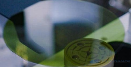
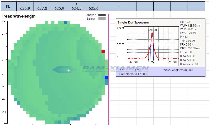
Test PL i El płytki diody elektroluminescencyjnej kwantowej przedstawiono na schemacie:
No. 2 GaAs based InGaP LED Epitaxy Wafer
GANW190724-INGAP
| Layer Name | Materialny | Grubość |
| P-cladding layer | P-AlInP | - |
| Warstwa aktywna | MQW | - |
| N-cladding layer | N-AlInP | 900nm |
| Bragg reflector | N-AlGaAs/AlAs | - |
| Warstwa bufora | N-GaAs | |
| podłoże | N-GaAs on-axis (100) plane without offcut |
No. 3 GaAs based LED Epitaxial Structure
GANWP19168-INGAP
| Layer Name | Materialny | Grubość |
| P-cladding layer | P-AlInP | - |
| Warstwa aktywna | MQW | - |
| N-cladding layer | N-AlInP | - |
| Warstwa bufora | N-GaAs | 300nm |
| podłoże | N-GaAs on-axis (100) plane without offcut |
2. FAQ of GaAs Light Emitting Diode Wafer
Q:We observed two MQW regions in GaInP LED wafer (GANWP19168-INGAP), illustrated in below figure. There are 9 pairs in each MQW separated by a thick barrier layer. May I know any reason to grow this kind of structure instead of a single stack of MQWs?
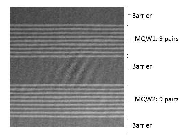
A: These are two groups of identical quantum wells in InGaP LED epitaxy. In order to increase the thickness of the active region and improve the reliability of the LED chip, the middle layer can be used normally without any influence on the photoelectric performance.
3. InGaP on GaAs for Light Emitting Diode Structure
InGaP, który wykazuje ogromny potencjał do zastąpienia materiałów zawartych w aluminium, jest krytycznym materiałem półprzewodnikowym zwykle hodowanym na podłożu GaAs. Jego właściwości są ściśle związane z warunkami wzrostu, takimi jak metoda wzrostu, temperatura podłoża, tempo wzrostu, orientacja podłoża, stosunek III/V itp. Tak więc InGaP jest idealny do hodowli heterostruktur do kilku zastosowań, takich jak czerwone diody LED o wysokiej jasności.
Atrakcyjność heterostruktury InGaP / GaAs wynika z jej ułożenia pasm, przesunięcie pasma walencyjnego (AEv = 0,24 – 0,40 eV) jest znacznie większe niż przesunięcie pasma przewodnictwa (Mc = 0,03 – 0,22 eV). Uważa się to za bardziej korzystne niż struktura pasmowa heterosystemu AlGaAs/GaAs.
InGaP to wysoce selektywne trawienie GaAs, które jest wykorzystywane jako warstwa zatrzymująca trawienie w naszej epitaksjalnej strukturze LED. Zwiększy to jakość i możliwości produkcyjne urządzeń z mikrodiodami elektroluminescencyjnymi. Ale warstwa zatrzymująca GaInP etch zwiększy wysokość bariery energetycznej, którą należy pokonać, gdy elektrony przepływają z kolektora do podkolektora. W tych warunkach wzmocnienie prądowe DC struktury diody LED MQW zmniejszy się. W związku z tym warstwa zatrzymująca trawienie InGaP powinna być wystarczająco cienka, aby zapewnić działanie urządzenia.
Aby uzyskać więcej informacji, prosimy o kontakt mailowy pod adresem sales@ganwafer.com i tech@ganwafer.com.