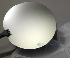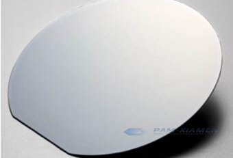
Estrutura de Diodo Emissor de Luz GaInP / AlInP
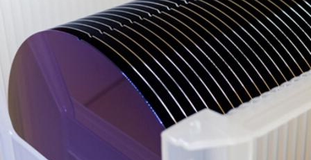
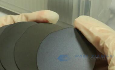
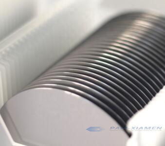
Light emitting diode (LED) structure with GaInP / AlInP epilayers can be offered by Ganwafer. The ternary InGaP and AlInP materials are lattice matched to GaAs susbtrate, which can be grown by MOCVD. Growing high quality III-V material semicondutor ternário is important to the fabrication of light emitting diodes, laser diodes and multi-junction photovoltaic. Light emitting diode structure with ternary GaInP and AlInP epilayers from Ganwafer is shown as follows:
1. GaAs Epi Estrutura do Diodo Emissor de Luz
No.1 GaAs LED Epitaxy
|
GaAs LED Structure (GANWP20065-LED) |
||
| Material da camada | Espessura | Nota |
| p-GaInP | - | Composition of In: 0.5;
mg dopado |
| p-GAP | - | |
| p-AlInP | - | |
| MQW | - | |
| n-AlInP | - | |
| DBR | - | |
| Parada de gravação n-GaInP | 20 nm | |
| Camada de buffer | - | |
| Subs GaAs. | 350 um | |
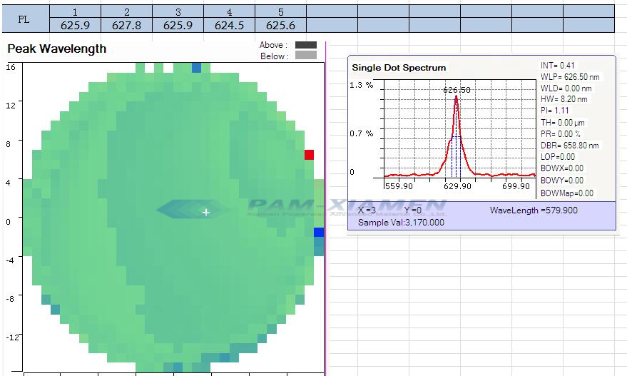
O teste PL e El da pastilha de diodo emissor de luz quântica é mostrado como o diagrama:
No. 2 GaAs based InGaP LED Epitaxy Wafer
GANW190724-INGAP
| Layer Name | Material | Espessura |
| P-cladding layer | P-AlInP | - |
| Active layer | MQW | - |
| N-cladding layer | N-AlInP | 900nm |
| Bragg reflector | N-AlGaAs/AlAs | - |
| Camada de buffer | N-GaAs | |
| Substrato | N-GaAs on-axis (100) plane without offcut |
No. 3 GaAs based LED Epitaxial Structure
GANWP19168-INGAP
| Layer Name | Material | Espessura |
| P-cladding layer | P-AlInP | - |
| Active layer | MQW | - |
| N-cladding layer | N-AlInP | - |
| Camada de buffer | N-GaAs | 300nm |
| Substrato | N-GaAs on-axis (100) plane without offcut |
2. FAQ of GaAs Light Emitting Diode Wafer
Q:We observed two MQW regions in GaInP LED wafer (GANWP19168-INGAP), illustrated in below figure. There are 9 pairs in each MQW separated by a thick barrier layer. May I know any reason to grow this kind of structure instead of a single stack of MQWs?
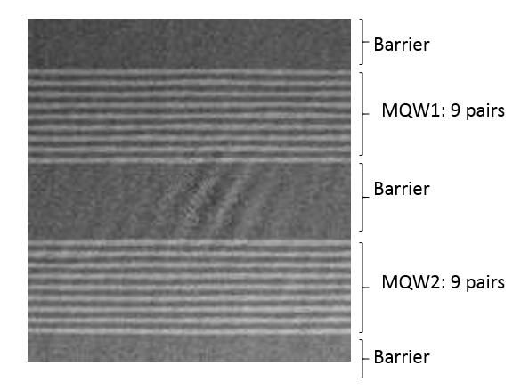
A: These are two groups of identical quantum wells in InGaP LED epitaxy. In order to increase the thickness of the active region and improve the reliability of the LED chip, the middle layer can be used normally without any influence on the photoelectric performance.
3. InGaP on GaAs for Light Emitting Diode Structure
O InGaP, que apresenta grande potencial para substituir os materiais contidos em alumínio, é um material semicondutor crítico geralmente cultivado em substrato de GaAs. Suas propriedades estão intimamente relacionadas às condições de crescimento, como método de crescimento, temperatura do substrato, taxa de crescimento, orientação do substrato, relação III/V, etc. Portanto, o InGaP é ideal para o cultivo de heteroestruturas para diversas aplicações, como LEDs vermelhos de alto brilho.
A atratividade da heteroestrutura InGaP/GaAs decorre de seu alinhamento de banda, o deslocamento da banda de valência (AEv = 0,24 – 0,40 eV) é significativamente maior que o deslocamento da banda de condução (Mc = 0,03 – 0,22 eV). Isto é considerado mais favorável do que a estrutura de bandas do sistema hetero AlGaAs/GaAs.
InGaP é um ataque altamente seletivo para GaAs, que é usado como a camada de parada de gravação em nossa estrutura epitaxial de LED. Isso aumentará a uformidade e a capacidade de fabricação de dispositivos de micro diodo emissor de luz. Mas a camada de etch stop GaInP aumentará a altura da barreira de energia que deve ser superada quando os elétrons fluem do coletor para o subcoletor. Sob esta condição, o ganho de corrente DC da estrutura do LED MQW diminuirá. Assim, a camada de etch stop do InGaP deve ser fina o suficiente para garantir o desempenho do dispositivo.
Para obter mais informações, entre em contato conosco pelo e-mail sales@ganwafer. com e tech@ganwafer. com.