Metal-organic Chemical Vapor Deposition (MOCVD) Technology
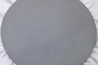
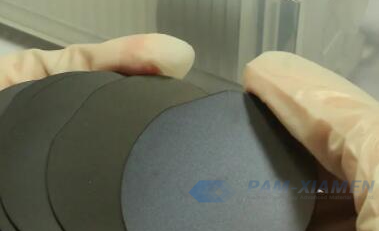
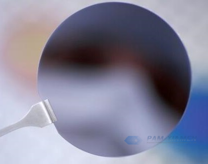
Metal-organic chemical vapor deposition (MOCVD) is a new vapor phase epitaxy growth technology developed on the basis of vapor phase epitaxy (VPE). MOCVD uses organic compounds of group III and group II elements and hydrides of group V and group VI elements as crystal growth source, and conducts vapor phase epitaxy on the substrate by thermal decomposition reaction to grow various III-V main groups, II-VI subgroup compound semiconductors and thin-layer single-crystal materials of their multicomponent solid solutions. Ganwafer can grow epiwafers, like III-V epiwafer, GaN epiwafer, SiC epi wafer and etc, by MOCVD technique.
1. Working Principle of MOCVD
Usually the MOCVD growth process is as follows: the reaction source material whose flow is precisely controlled is passed into the reaction chamber of quartz or stainless steel under the carrier gas (usually H2, some systems use N2), and the epitaxial layer is grown after the surface reaction occurs on the substrate. The substrate is placed on a heated base. The tail gas remaining after the reaction is swept out of the reaction chamber and discharged from the system after passing through a tail gas treatment device that removes particulates and toxicity. The working principle of MOCVD is shown in the figure:
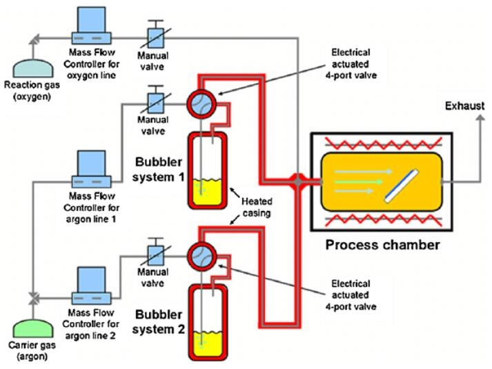
Working Principle of MOCVD System
2. MOCVD Technology Superiority
Compared with other epitaxial growth techniques, MOCVD technology has the following advantages:
1) The components and dopants used for the growth of compound semiconductor materials are introduced into the reaction chamber in a gaseous manner. Therefore, the composition, doping concentration, thickness, and etc. can be controlled by precisely controlling the flow and on-off time of the gaseous source to grow thin and ultra-thin layer materials.
2) The gas flow rate in the reaction chamber is faster, suitable for the growth of heterostructures and superlattice and quantum well materials.
3) The crystal growth is carried out in the form of pyrolysis chemical reaction, which is epitaxial growth in a single temperature zone. As long as the uniformity of the reaction source gas flow and temperature distribution is well controlled, the uniformity of the epitaxial material can be guaranteed. Therefore, it is suitable for epitaxial growth of multiple sheets and large sheets, and is convenient for industrialized mass production.
4) Usually, the crystal growth rate is proportional to the flow rate of the III source, so the growth rate can be adjusted in a wide range. Faster growth rates are suitable for batch growth.
5) The structure of the reaction chamber is relatively simple due to the low requirement for vacuum degree.
In fact, the most attractive part of MOCVD technology is its versatility. As long as a suitable metal organic source can be selected, epitaxial growth can be carried out. Moreover, as long as the uniform distribution of air flow and temperature is ensured, a large area of uniform material can be obtained, which is suitable for large-scale industrial production.
3. Specific Applications of Metal-Organic Chemical Vapor Deposition
After nearly 20 years of rapid development, MOCVD has become one of the key technologies for the preparation of semiconductor compound materials. In order to meet the needs of the development of microelectronics and optoelectronic technology, GaAlAs/GaAs, GaInP/GaAs, InAs/InSb, InGaN/GaN, AlGaN/GaN, GaInAsP/InP, AlGaInAs/GaAs and other thin films are prepared by MOCVD.
The development of MOCVD technology is closely related to the demand for compound semiconductor material research and device fabrication, which in turn promotes the development of new devices. At present, MOCVD technology is used in the fabrication of various main types of compound semiconductor devices, including: HEMT, PHEMT, HFET, HBT, quantum well laser, vertical cavity surface laser, LEDs and so on.
For more information, please contact us email at sales@ganwafer.com and tech@ganwafer.com.