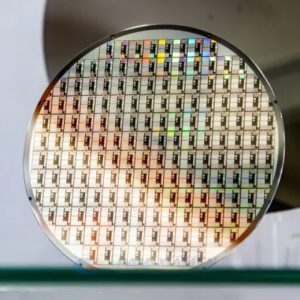
Ganwafer a leading epitaxy foundry of epi wafer and material solutions focuses on epitaxial growth services for semiconductor manufacturing. We design structures for epitaxial growth and manufacture of compound semiconductor epitaxial wafers. Our epi services are used in electronic and photonic device. As for epitaxial process, we provide III-V Epi service (such as RF epitaxial wafer and Photonics epitaxial wafer) based on GaAs Substrate, InP substrate, GaSb Substrate, InAs Substrate, InSb substrate, or in different types of epi on bare substrates with buried layers by MBE or MOCVD. Our excellent epitaxial technologies deliver low to a high concentration for both n-type and p-type, superior specification epi for R&D, and epi specified for mass production.
Notre semi-conducteur épitaxial III-V avec homoépitaxie et hétéroépitaxie par les technologies de dépôt épitaxial MOCVD, MBE ou CVD, y compris SiC sur SiC, GaN sur silicium/SiC/saphir, et épitaxie III-V sur GaAs/InP/InAs/GaSb/Silicium. Et les tailles de plaquettes III-V basées sur nos services de traitement par épitaxie peuvent atteindre 50,8 mm, 76,2 mm, 100 mm, 150 mm et 200 mm.