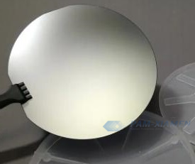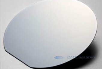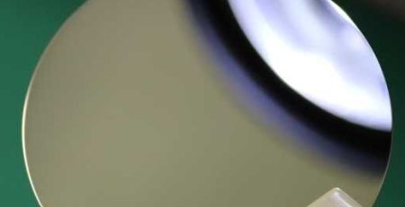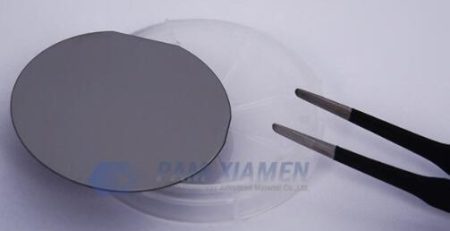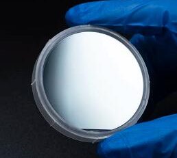
GaAs Epi Wafer by MBE for Edge Emitting Laser (EEL)
808nm, 980nm or 9XXnm GaAs (gallium arsenide) epi wafer is used in edge emitting laser (EEL) for industrial welding, photolithography, medical applications, distance measurement offered by Ganwafer, one of leading epitaxial wafer manufacturers.
1. Fabrication of EEL on GaAs Epi Wafer
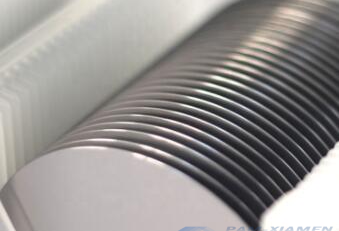
GaAs based EEL epitaxial wafer can use molecular beam epitaxy (MBE) to manufacture edge emitting diode lasers. When the cover layer is deposited vertically to form the structure, the semiconductor epitaxial GaAs films is patterned and the thickness is precisely controlled.
After patterning of the GaAs-based MBE epitaxial layers and MBE deposition, top contacts are deposited for both structures. The next step is to cut the epi wafer. For edge-emitting diodes, the laser can be completely generated only after cutting the wafer. Therefore, edge-emitting lasers cannot be tested during the growth process. The cutting process of GaAs epiwafer is very important for edge-emitting lasers, and irregularities of GaAs EEL epitaxial wafers can reduce yield and reliability. Generally, the EEL GaAs double heterostructure will limits the formed carriers (electrons and holes) in a narrow region and serve as waveguide for optical field. This structure will make low threshold pump power and high efficiency for the laser.
2. About Edge Emitting Laser
There are two main types of EEL: a) FP laser; b) DFB laser:
In the FP laser, the laser diode is a laser, and its reflective mirror is just a flat cracked surface at the end of the laser chip. FP laser is mainly used for low data rate and short distance transmission. The transmission distance is generally within 20km, and the speed is within 1.25G;
The DFB laser diode based on epitaxial GaAs wafer is a laser with a grating structure in the cavity, which generates multiple reflections in the entire cavity. DFB lasers on photonic crystal laser epi wafer are mainly used for long-distance transmission at high data rates.
Edge-emitting lasers on GaAs epi wafer have completely changed the laser system and endowed it with new special properties, such as miniaturization, stable coherent light and narrow emission wavelengths. In practice, GaAs based EEL can be used as a direct laser, but it can also be coupled with a fiber or crystal to make a fiber laser or DPSSL. This advanced laser technology provides specific advantages, such as better beam quality, improved laser noise stability, and higher power output.
For more information, please contact us email at sales@ganwafer.com and tech@ganwafer.com.