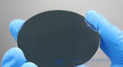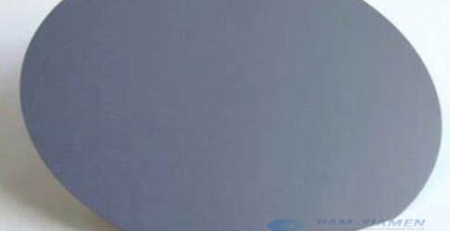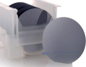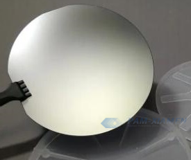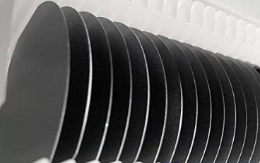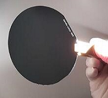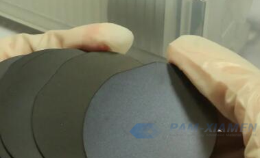
650V GaN FETs Chip for Fast Charge
Ganwafer can offer 650V GaN FETs Chip for fast charge products for the consumer market. GaN FETs advantages in the charger are mainly reflected in: small size, light weight, high power density, high efficiency but not easy to heat. Moreover, mobile phones, notebooks can be charged by the GaN FETs Chip, which is compatible with multiple devices.
1. 650V GaN FET Datasheet
1.1 GaN FET 650V Chip Absolute Maximum Ratings (TC=25°C unless otherwise stated)
| Symbol | Parameter | Limit value | Unit | |
| VDSS | Drain to source voltage | 650 | V | |
| VDSS | Gate to source voltage | 一25~+2 | ||
| ID | Continuous drain current @TC=25°C | 15 | A | |
| Continuous drain current @TC=100°C | 10 | |||
| IDM | Pulse drain current | 65 | A | |
| PD | Maximum power dissipation @ TC=25°C | 65 | W | |
| TC | Operating temperature | Case | 一55~150 | °C |
| TJ | Junction | 一55~175 | °C | |
| TS | Storage temperature | 一55~150 | °C | |
1.2 650V GaN FETs Chip Electrical Parameters (TJ=25°C unless otherwise stated)
| Symbol | Parameter | Min | Typ | Max | Unit | Test Conditions |
| Forward Device Characteristics | ||||||
| V(BL)DSs | Drain-source voltage | — | 650 | — | v | Vcs=-25V |
| Vasth) | Gate threshold voltage | — | -18 | — | v | VDs=Vas,IDs=luA |
| RDS(on) | Drain-source on-resistance | — | 150 | 180 | mQ | Vcs=OV,ID-10A |
| — | — | — | VGs=OV, ID-10A,TJ=150’C | |||
| lDss | Drain-to-source leakage current |
— | — | 3 | uA | VDs=650V,VGs=-25V |
| — | — | 30 | VDs=400V,VGs=-25V, T=150’c |
|||
| lass | Gate-to-source forward leakage current |
— | 3.7 | 100 | nA | VGs=2V |
| Gate-to-source reverse leakage current |
— | -3.5 | -100 | VGS=-25V | ||
| CIss | Input capacitance | — | 650 | — | pF | vGs=-25V,VDS=300V,f=1MHz |
| Coss | Output capacitance | — | 40 | — | ||
| CRSS | Reverse capacitance | — | 10 | — | ||
| QG | Total gate charge | — | 9 | — | nC | VDS=200V,VGS=-25V to ov, ID=10A |
| QGS | Gate-source charge | — | 2 | — | ||
| QGD | Gate-drain charge | — | 7 | — | ||
| tn | Reverse recovery time | — | 4 | — | ns | Is=0A to 11A,VDD=400V di/dt=1000A/uS |
| Q. | Reverse recovery charge | — | 17 | — | nC | — |
| TIX(on) | Turn-on delay | — | 0.5 | — | — | VDs=200VVG=-25V to ov, ID=10A |
| tR | Rise time | — | 9 | — | ||
| tD(off) | Turn-off delay | — | 0.5 | — | ||
| tF | Fall time | — | 10 | — | ||
| Reverse Device Charactcristics | ||||||
| VSD | Reverse voltage | — | 7 | — | v | VGS=-25V,Is=10A,Tc=25′ C |
2. Why is Gallium Nitride the Best Choice for Fast Charging Materials?
As one of the core materials of third-generation semiconductors, GaN has three main characteristics:
- high switching frequency
- large band gap
- lower on-resistance.
As large-screen mobile phones have become the mainstream and processors have been continuously upgraded, battery technology has reached a bottleneck. Therefore, how to charge faster has become the key to solving the problem of battery lifetime. Gallium nitride (GaN) has attracted attention for two main reasons: the screen size continues to rise, and the battery capacity continues to rise. In the future, the larger the smart phone screen, the entire CPU, radio frequency and peripheral electronic devices will use the power part, and the battery will become larger and larger.
The charger fabricated on GaN FET high voltage chip is very small, but with a very high charging efficiency, low heat generation. The speed of the GaN charger chip is twice as fast as the original one.
3. What is the Difference Between GaN (Gallium Nitride) and Traditional Silicon Materials?
GaN FET devices are that they has higher efficiency, smaller size and lighter weight than that on silicon. Specifically, GaN runs 20 times faster than silicon, and can achieve three times higher power, and at least double the energy density. Compared with the traditional power management method AC/DC, the efficiency is improved by at least 3 points.
The appearance of gallium nitride has changed the status quo that the size of the charger continues to increase with the increase of power density. It is currently the fastest power switching device in the world and can maintain a high efficiency level under the premise of high-speed switching. The high switching frequency reduces the size of the transformer, thereby greatly reducing the size of the charger. At the same time, gallium nitride has lower loss. After using GaN FET power chip, it reduces the use of other components and further reduces the size of the charger.
With the development of artificial intelligence and 5G communications, high requirements have been placed on the GaN FET technology in fast charging of 5G mobile phones, notebook computers and other smart terminals. As users demand versatility and portability of chargers, thN e GaN FET market in 650V fast charging market has grown rapidly. As a one of GaN FET manufacturers, Ganwafer is actively deploying GaN FETs chip component design and production capacity.
For more information, please contact us email at sales@ganwafer.com and tech@ganwafer.com.