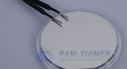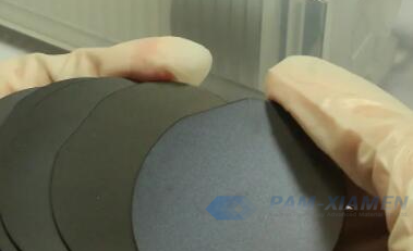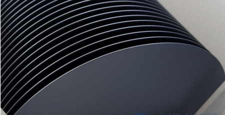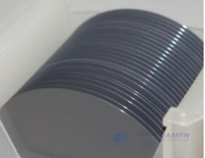
AlGaAs / GaAs Heterostructure
AlGaAs / GaAs heterostructure can be offered by Ganwafer. Aluminum gallium arsenide (AlGaAs), as an important optoelectronic basic material, is widely used in high-speed electronic devices and infrared detectors. The quality of the AlGaAs material, especially the quality of the surface directly affects the optoelectronic properties of the fabricated device. More details of AlGaAs / GaAs heterostructure semiconductor wafer for sale are shown as follows:
1. AlGaAs / GaAs Heterostructure
No. 1 AlGaAs Bragg Stack Wafers
GANW201123-ALGAAS
| Layer | Material | Repeat | Thickness (nm) | Note |
| 11 | Al0.2Ga0.8As | 5 | – | Alternating layers 10/11 |
| 10 | Al0.63Ga0.37As | 5 | – | |
| 9 | Al0.2Ga0.8As | – | ||
| 8 | Al0.63Ga0.37As | – | ||
| 7 | Al0.2Ga0.8As | – | ||
| 6 | Al0.43Ga0.57As | – | ||
| 5 | Al0.2Ga0.8As | 400 | ||
| 4 | Al0.63Ga0.37As | – | ||
| 3 | Al0.2Ga0.8As | – | ||
| 2 | Al0.63Ga0.37As | 5 | – | Alternating layers 1/2 |
| 1 | Al0.2Ga0.8As | 5 | – | |
| 0 | GaAs wafer |
No. 2 AlGaAs / GaAs Heteroepitaxial Wafer
GANW200710-ALGAAS
2” size AlGaAs / GaAs Wafer:
280nm AlGaAs (undoped, crystal axes orientation [100], 20% Al)
100nm Al0.52In0.48P (Al composition would be a little tolerance)
GaAs substrate
Note:
If you just need the AlGaAs thin film for your applications, HCl solution could be used here to separate the AlGaAs and GaAs substrate by dissolving AlInP.
No. 3 AlGaAs Epi Stacked on GaAs Substrate
GANW191009 – ALGAAS
| Layer | Type | Material | Group | Repeat | Thickness | Dopant | Mole Fraction (x) | Strain (ppm) | PL (nm/eV) | CV Level |
| 10 | i | GaAs | – | |||||||
| 9 | i | Al(x)GaAs | 100±5% Å | 0.40±5% | ||||||
| 8 | N+ | Al(x)GaAs | – | Si | – | – | ||||
| 7 | i | Al(x)GaAs | – | – | ||||||
| 6 | i | GaAs | – | |||||||
| 5 | i | GaAs | – | – | – | |||||
| 4 | i | Al(x)GaAs | 1 | – | – | – | ||||
| 3 | i | GaAs | 5000±5% Å | |||||||
| 2 | i | Al(x)GaAs | – | – | ||||||
| 1 | i | GaAs | – | |||||||
| 0 | Substrate |
Remark: concentration tolerance: +/-20%
No. 4 AlGaAs / GaAs Epitaxial Wafer
GANW180412-ALGAAS
| Layer Name | Material | Thickness, um | Conductivity Type | Concentration cm¯³ | |
| H1 | Contact layer | GaAs | 0.070 | – | 5Χ10¹⁸ |
| H2 | Gradient layer 2 | GaAs | – | – | – |
| – | |||||
| H3 | Transition layer 2 | GaAs | – | – | – |
| H4 | Gradient layer 1 | Al₀.₂₃Ga₀.₇₇As | 0.025 | – | – |
| – | |||||
| H5 | Donor layer | Al₀.₂₃Ga₀.₇₇As | – | n+ | – |
| H6 | Spacer | Al₀.₂₃Ga₀.₇₇As | – | – | 5Χ10¹⁴ |
| H7 | Transition layer 1 | GaAs | – | Pi | – |
| H8 | Channel layer | InxGa1-xAs | – | – | – |
| H9 | Buffer layer 2 | GaAs | 0.2 | – | – |
| H10 | Superlattice | Al₀.₂₃Ga₀.₇₇As /GaAs | – | – | – |
| H11 | Buffer layer 1 | GaAs | – | – | 5Χ10¹⁴ |
| H12 | Substrate | GaAs | 450±10 | i | ₋ |
Reamrks:
The thickness and doping level of the contact layer n+-GaAs can be specified by the consumer within 0.01~0.15 um and 1×10¹⁸~6Χ10¹⁸ cm-³, respectively.
2. About AlGaAs Material
Aluminum gallium arsenide (AlGaAs) material, as a typical representative of III-V compound semiconductors, has been widely studied and applied due to its high carrier mobility, tunable composition, and similar lattice to GaAs. One of the typical applications is the use of molecular beam epitaxy of GaAs / AlGaAs heterostructure growth to modulate doped two-dimensional electron gas materials. High-speed microelectronic devices (HEMT, PHEMT) based on high-quality two-dimensional electron gas structure, such as high electron mobility transistors, are widely used in ultra-high-speed, ultra-high-frequency, low-noise microelectronic devices and circuits.
At the same time, it has many potential applications in sensors and new lasers used in next-generation optical communication and data transmission. Therefore, the requirements for the preparation quality of AlGaAs thin films, AlGaAs quantum dots, and AlGaAs quantum wells are getting higher and higher, just like the preparation technology requirements of Si materials are getting higher and higher with the progress of microelectronics technology. In addition, the research on the growth process and surface microstructure of high-quality AlGaAs with different compositions is of great significance for the growth of high-quality superlattices. Therefore, fundamental research work on AlGaAs surfaces is valuable.
AlGaAs materials have the advantage of being easy to integrate laser diodes and other optical devices, which enable AlGaAs / GaAs heterostructure laser with highly integrated designs of ultra-small size, which can effectively reduce the size and weight of components to meet practical applications.
For more information, please contact us email at sales@ganwafer.com and tech@ganwafer.com.