Homoepitaxy of N-Type Undoped InAs on InAs (001) Substrate
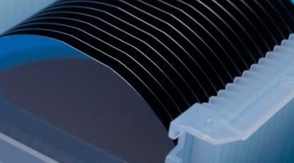
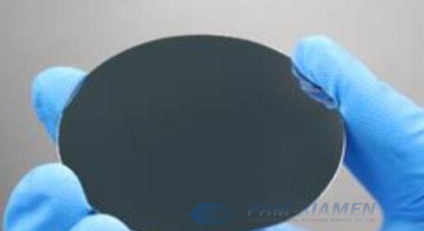
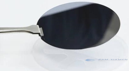
Indium arsenide (InAs) wafer material has great potential for fabricating different devices since its high electron mobility, narrow bandgap, high carrier concentration, and lattice-matched systems (InAs, GaSb, AlSb, and their alloys) at 6.1 A˚. Homoepitaxial InAs layer with different doping concentration on InAs (001) substrate can be used to manufacture avalanche photodiodes and photodetectors. InAs thin films with highly n-type doped, lightly doped or undoped are usually deposited as layers of plasmon-cladding and waveguide-space, which are for interband cascade laser and mid IR quantum cascade to help extend the wavelength. Homoepitaxy of InAs (001) can be offered by Ganwafer as below:
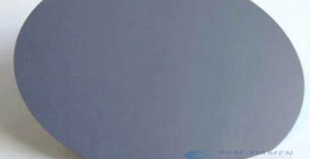
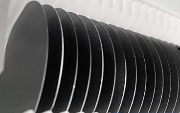
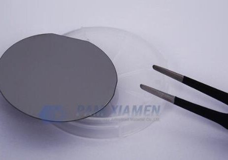
1. InAs Homoepitaxial Structure
GANW200115-INAS
| Layer | Type/Dopant | Carrier concentration (cm-3) | Thickness (um) |
| InAs(001) | n-type/Undoped | <2 x 1016 cm-3 | 2-2.5 |
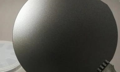
| 2-inch n-type InAs (001), heavily doped substrate ((5-50)x1017 cm-3), backside polished | |||
The plasma frequency of highly doped InAs is controllable in a wide mid-infrared frequency range, so the InAs homoepitaxy is ideal for metamaterial structure and mid-IR plasmonic. With the wide applications of InAs (001) homoepitaxy, to facilitate the development of high-performance devices, the demands for high quality epilayer with low defect density and atomically smooth surface are increasing. It is important for complicated devices, such as QC and IC lasers.
2. Surface Morphology and Defect Densities of InAs Homoepitaxy Epilayer
Surface morphology and defect densities are important metrics that shows the quality of InAs thin film. The homoepitaxy InAs is highly doped with smooth surface that demonstrates the waveguide layer grown at high quality crystalline, contributing to sharp interfaces in the laser structure fabrication later. The structure is composed of untral thin layers up to 100 in interband / quantum cascade devices.
For InAs homoepitaxial growth, low defect density is critical since it can penetrate into the laser structure and become recombination center to degrade the performance of laser. Therefore, smooth surface morphology and low defect density are very important for realizing perfect performance of devices. To ensure the wafer quality, we can use SEM, AFM, and DIC microscopy to observe the homoepitaxial InAs layer after epitaxial growth process, and then optimize the conditions for growth of homoepitaxial InAs layer on InAs (001) substrate.
For more information, please contact us email at sales@ganwafer.com and tech@ganwafer.com.