InAs / GaSb Type II Superlattice (T2SL) Structure
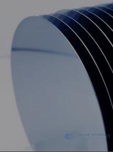
Ganwafer can offer GaSb epitaxial wafer with type II superlattice (T2SL) structure. T2SL is a III-V group 6.1Å Sb-based material composed of InAs (6.0583 Å), GaSb (6.09593 Å) and AlSb (6.1355 Å) whose lattice constants are close to each other and their compounds are periodically stacked according to a certain layer thickness, composition and order. Due to the small lattice mismatch between them, complex binary or ternary compounds can be grown. The energy gap of Sb-based materials and related compounds ranges from 0.41eV (InAs) to 1.70eV (AlSb). More details of GaSb-based type 2 strained layer superlattice structure please see as follows:
1. InAs / GaSb T2SL Structure
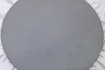
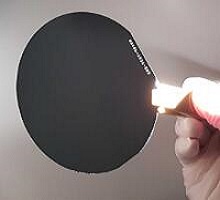
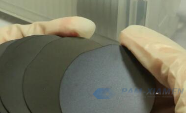
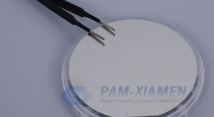
GANW200622-T2SL
| Growth of T2SL structure | ||||
| Layer Details | Layer Material | Thickness / No of Monolayers (ML) | Doping Type / Doping Concentration | No of Periods |
| 1st Layer: Buffer layer | GaSb | 800nm | p+-type / Be: 1 x1018 cm-3 | Single Layer |
| 2nd Layer: 0.5µm thick n+ type, M Barrier region | InAs | – | Un-doped | ~111periods |
| GaSb | – | – | ||
| 3rd Layer: 2.2µm thick slightly p-type doped (Be doping temperature: 760°C), π region | InAs | – | – | ~330periods |
| GaSb | – | – | ||
| InSb | – | – | ||
| 4th Layer: 0.5µm thick slightly doped n-type doped, M-region | InAs | – | – | ~54periods |
| GaSb | – | – | ||
| AlSb | – | – | ||
| GaSb | 5ML | – | ||
| 5th Layer: 0.5µm thick n+ type, M Barrier region | InAs | – | – | ~54periods |
| GaSb | – | Un-doped | ||
| AlSb | – | – | ||
| GaSb | – | – | ||
| 6th Layer: Cap & Top contact layer | InAs | – | n+-type / – | Single Layer |
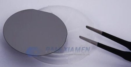
Substrate:3 inch GaSb (001) Substrate (n-type doped / Te: E16)
2. About InAs/GaSb Type II Superlattice
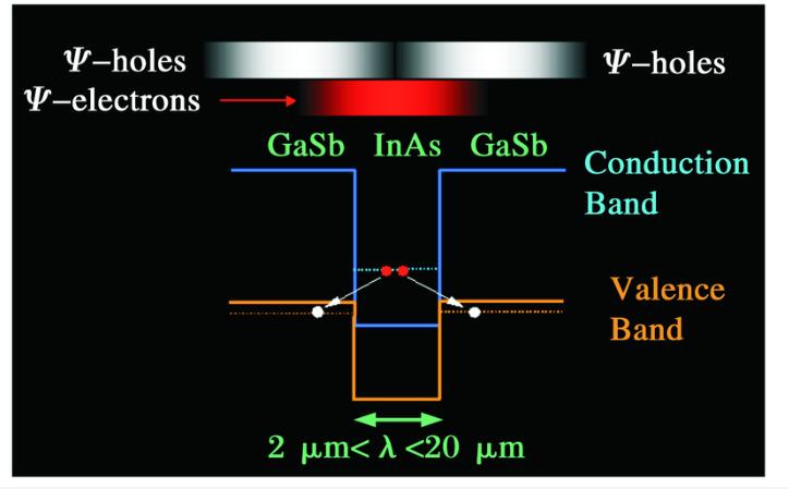
The InAs / GaSb T2SL material, which has type II band structure, is formed by stacking InAs thin films and GaSb thin films according to different arrangement periods. At the interface between the InAs and GaSb layers, the top of the conduction band of the InAs layer is about 150 meV lower than the bottom of the valence band of the GaSb layer, thus forming a type-II heterojunction structure. The forbidden band width of the T2SL material is formed by the band gap between the bottom of the electron microstrip (C1) and the top of the first heavy hole microstrip (HH1) in the Brillouin zone. Depending on the thickness and arrangement of the films, theoretically, the forbidden band width of type 2 superlattice can be continuously adjusted between 0 and 400 meV, as shown in Figure below:
Energy Band Structure of InAs / GaSb Superlattice
3. Applications of Type II Superlattice Technology
Sb-based stressed layer superlattice (SLS), especially type II superlattice (T2SL) materials, has a wide range of applications in detectors, lasers, and modulators, especially in the field of infrared detection. Due to the great potential and advantages, it is generally believed that T2SL material can replace the current mainstream HgCdTe (MCT) material. High-quality InAs / GaSb type II superlattice materials have been grown by molecular beam epitaxy (MBE) technology, and high-performance type II superlattice infrared detectors covering the entire infrared band have been successfully developed.
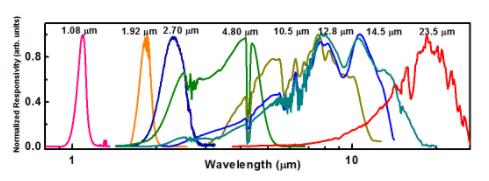
T2SL Infrared Detector Covering All Band Infrared Frequency
4. Advantages of InAs / GaSb T2SL
The valence band of GaSb is higher than the conduction band of the InAs material. As a result, the InAs and GaSb layers separated in real space form a conduction band potential well and a valence band potential well, respectively. Electrons and holes are confined in the InAs and GaSb layers, respectively. On the other hand, the effective mass of electrons is light, and the electron wave functions pass through the overlap of the barrier layers to form a microstrip structure. The transitions of carriers caused by the action of external infrared radiation belong to the interband transitions. This special band structure enables type II semiconductor superlattice materials to have the following advantages:
1) Inter-band transitions can absorb normal incidence and have high quantum efficiency;
2) By adjusting the strain and its energy band structure, the separation of heavy and light holes is large, the Auger recombination and related dark currents are reduced, and the operating temperature of the type-ii superlattice focal plane array is increased;
3) The effective mass of electrons is large, which is three times that of HgCdTe (for T2SL, the electron mass is me≈0.03 m0; for HgCdTe, the electron mass is me≈0.01 m0). The tunneling current is small, and high detection rate can be obtained, especially in ultra-long wave;
4) Adjustable band gap, adjustable response wavelength from short wave to 30 um, can prepare short wave, medium wave, long wave, ultra long wave, two-color and multi-color devices;
5) Based on III-V Material growth technology, large-area material uniformity is good, and the cost is low. Using MBE for type-2 strained-layer superlattice growth has a high degree of design freedom, easy doping control, no alloy fluctuations and cluster defects, and good focal plane detector uniformity.
For more information, please contact us email at sales@ganwafer.com and tech@ganwafer.com.