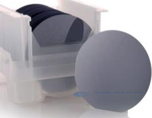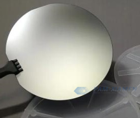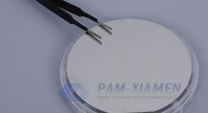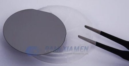
Extended InGaAs Wafer on InP Substrate
Indium gallium arsenide (InGaAs) wafer is a ternary compound semiconductor, which is suitable for detector applications. The InGaAs is lattice matched to InP substrate, and InGaAs epi wafer based on InP substrate can response the wavelength from 900 nm to 1700 nm. Moreover, the wavelength can be extended to 2600 nm to meet the space remote sensing needs when increase the In composition at 0.83. Extended InGaAs wafer from Ganwafer can be to fabricate detectors sensitive above 1600 nm up to 2000 nm. More detailed specification of III-V epi wafer with InGaAs active layer please see below:
1. InP-based InGaAs Epitaxial Structure
GANW200114-INGAAS
| # | Material | Doping | N(#/cm3) | Thickness(nm) |
| 8 | InP | p | – | – |
| 7 | InGaAs | – | 1E19 | – |
| 6 | InP | – | – | – |
| 5 | Extended InGaAs | NID | – | – |
| 4 | InP | – | – | 100 |
| 3 | InGaAs | – | – | – |
| 2 | InP | – | 1E14 | – |
| 1 | InGaAs | – | – | – |
| InP S.I. Substrate 300 um | ||||
Note:
Layer 5 can be standard InGaAs or strained InGaAs. With strained InGaAs, the wavelength of InP based epitaxial wafer should be 1750nm, 2000nm max. If >1750nm, there would be mis-match dislocation line. The dislocation line does not affect InGaAs wafer itself, but affect dark current. The dark current of the device would be bigger a little.
2. Mis-Match Dislocation Line of InP-Based InGaAs Wafer
When the In content x is greater than 0.53, the lattices of InxGa1-xAs and the InP substrate will no longer match, and the lattice mismatch between the two will increase with the increase of In content. The introduction of dislocation line leads to the formation of many defects. The dislocation line does not affect wafer itself, but seriously affects the dark current of InGaAs detector. The problem of extremely low dark current is one of the bottleneck problems restricting the development of photoelectric detection systems in the aerospace field. The solution of this problem strongly depends on the discovery of new materials and breakthroughs in material properties. Therefore, it is of great significance to carry out basic research on near-infrared core detection materials, and to explore new phenomena, new effects and aerospace adaptability in the process of moving from materials to devices.
3. Strained InGaAs / InP Quantum Well Technology
As the most widely used active region of semiconductor lasers, InGaAs / InP quantum wells exhibit quantized sub band and step state density inside, which will greatly improve the threshold current density and temperature stability of lasers. By changing the potential well width and potential barrier height, the quantized energy interval can be changed, and the tunable characteristics of the laser can be realized. Compared with the traditional double heterojunction semiconductor laser, the threshold current of the laser can be effectively reduced, and improve the quantum efficiency and differential gain. The introduction of strain into the quantum well will significantly change its own energy band structure, and by adjusting the positions of the heavy and light hole bands in the valence band, the design parameters and degrees of freedom of the InGaAs semiconductor epitaxial structure of the chip are increased.
Generally speaking, the introduction of compressive strain in the in InGaAs wafer will aggravate the change of the energy band function, thereby reducing the threshold current of the laser; while the introduction of tensile strain will smoothen the energy band function and improve the gain of the material under high power to a certain extent. The emergence of strained quantum wells makes it possible to obtain the desired energy band structure and increase the gain by adjusting the strain, which makes a great leap in the performance of semiconductor lasers.
For more information, please contact us email at sales@ganwafer.com and tech@ganwafer.com.