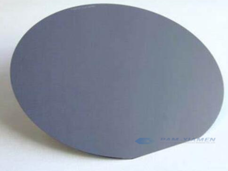
GaInP / AlGaInP Laser Diode Structure
III-V compound semiconductor laser diode structures have been developed for more than half a century and their wavelength coverage ranges from deep ultraviolet to far infrared, and their output power ranges from milliwatts to kilowatts. For example, the emission wavelength range of GaAs-based devices is about 610~1300nm, it is the core light source of red light for laser display, high-power semiconductor laser and 850nm data communication. The lasing wavelength range of InGaP / AlGaInP quantum well laser is 610-700nm, which is mainly used in laser display and other fields. The laser diode structure with GaInP well can be provided as below, as well as customized laser diode stack can be grown by Ganwafer:
1. GaAs Laser Diode Structure
| GaInP / AlGaInP Wafer Structure, Red Light (GANW200311-GAINP) | |||||
| Layer | Material | Concentration | Dopant | Thickness | |
| 10 | P-Contact | GaAs | – | p-Zn Doped | – |
| 9 | Cladding | AlGaInP | 1×10¹⁸ | p-Zn Doped | – |
| 8 | waveguide | AlGaInP | – | – | – |
| 7 | Barrier | AlGaInP | – | – | – |
| 6 | 1x Quantum Well | GaInP Well (0.65um PL) | – | – | – |
| 5 | Barrier | AlGaInP | – | – | 10 |
| 4 | waveguide | Al0.1Ga0.4In0.5P | – | – | – |
| 3 | Cladding | AlGaInP | – | N Si Doped | – |
| 2 | Buffer | GaAs | 5×10¹⁸ | N Si Doped | – |
| 1 | Substrate | N-doped GaAs Substrate | |||
2. GaInP / InGaAlP Quantum Well
GaInP is a highly efficient light-emitting material. AlGaInP / GaInP multi-quantum well (MQW) epitaxial wafers are the most important materials for realizing red light emission. InGaP / InGaAlP diode laser structure has a series of advantages such as small threshold value, good monochromaticity and high output power, but their monochromaticity and output wavelength are slightly affected by voltage and temperature, and this instability will have a certain impact on their application range. Therefore, the laser diode fabricated on InGaP / InGaAlP MQW should work in a constant voltage state as much as possible to ensure better output characteristics.
In terms of InGaP / InAlGaP laser diode structure materials, doping more Al in the active layer shortens the emission wavelength, and defects related to oxygen will severely decrease their efficiency. Furthermore, the band offset between the energy band shift between the quantum well and the potential barrier will lead to low carrier confinement and large carrier leakage current of the laser diode.
A new strain-induced quantum well intermixing (QWI) technique is proposed based on InGaP / InAlGaP red semiconductor laser structure, which will cause bandgap blueshift to some extent. Researchers found that the bandgap blushift of InGaP / InAlGaP material system can reach as large as 250 meV (75 nm)at wavelength of about 640 nm through optimizing the temperature, duration and cycle of annealing. QWI technology may be a good solution for producing high efficiency AlGaInP laser diode structure at short wavelength of yellow and orange.
For more information, please contact us email at sales@ganwafer.com and tech@ganwafer.com.

