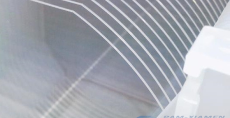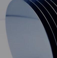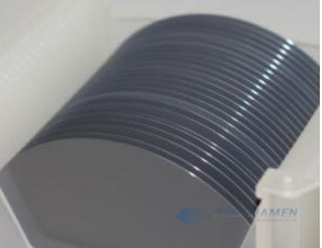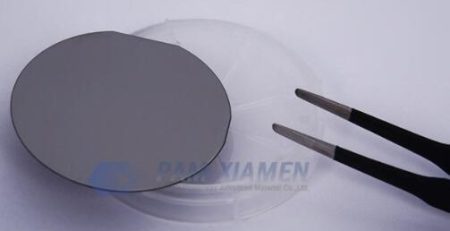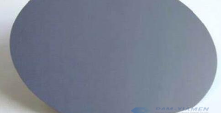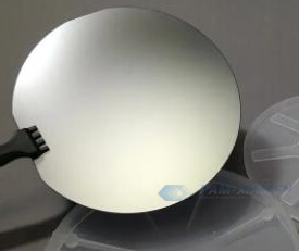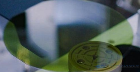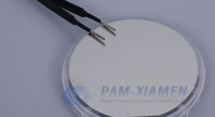
InP Substrat üzerinde Genişletilmiş InGaAs Gofret
Indium gallium arsenide (InGaAs) wafer is a ternary compound semiconductor, which is suitable for detector applications. The InGaAs is lattice matched to InP substrate, and InGaAs epi wafer based on InP substrate can response the wavelength from 900 nm to 1700 nm. Moreover, the wavelength can be extended to 2600 nm to meet the space remote sensing needs when increase the In composition at 0.83. Extended InGaAs wafer from Ganwafer can be to fabricate detectors sensitive above 1600 nm up to 2000 nm. More detailed specification of III-V epi gofretInGaAs aktif katmanı ile lütfen aşağıya bakın:
1. InP tabanlı InGaAs Epitaksiyel Yapı
GANW200114-INGAAS
| # | Malzeme | Doping | N(#/cm3) | Kalınlık (nm) |
| 8 | InP | p | - | - |
| 7 | InGaAs | - | 1E19 | - |
| 6 | InP | - | - | - |
| 5 | Genişletilmiş InGaAs | NID | - | - |
| 4 | InP | - | - | 100 |
| 3 | InGaAs | - | - | - |
| 2 | InP | - | 1E14 | - |
| 1 | InGaAs | - | - | - |
| InP SI Yüzey 300 um | ||||
Not:
Katman 5, standart InGaAs veya gergin InGaAs olabilir. Gerilmiş InGaAs ile, InP tabanlı epitaksiyel levhanın dalga boyu 1750nm, maksimum 2000nm olmalıdır. >1750nm ise, yanlış eşleşme dislokasyon çizgisi olacaktır. Dislokasyon çizgisi InGaAs gofretinin kendisini etkilemez, ancak karanlık akımı etkiler. Cihazın karanlık akımı biraz daha büyük olurdu.
2. InP-Tabanlı InGaAs Gofretinin Yanlış Eşleşme Çıkığı Çizgisi
In içeriği x 0,53'ten büyük olduğunda, In'in kafeslerixga1-xAs ve InP alt tabakası artık eşleşmeyecek ve ikisi arasındaki kafes uyumsuzluğu, In içeriğinin artmasıyla artacaktır. Dislokasyon hattının devreye girmesi birçok kusurun oluşmasına neden olur. Dislokasyon çizgisi gofretin kendisini etkilemez, ancak InGaAs dedektörünün karanlık akımını ciddi şekilde etkiler. Son derece düşük karanlık akım sorunu, havacılık alanında fotoelektrik algılama sistemlerinin geliştirilmesini kısıtlayan darboğaz sorunlarından biridir. Bu sorunun çözümü büyük ölçüde yeni malzemelerin keşfedilmesine ve malzeme özelliklerinde çığır açan gelişmelere bağlıdır. Bu nedenle, yakın kızılötesi çekirdek algılama malzemeleri üzerinde temel araştırma yapmak ve malzemelerden cihazlara geçiş sürecinde yeni fenomenleri, yeni etkileri ve havacılık uyarlanabilirliğini keşfetmek büyük önem taşımaktadır.
3. Süzülmüş InGaAs / InP Kuantum Kuyusu Teknolojisi
As the most widely used active region of semiconductor lasers, InGaAs / InP quantum wells exhibit quantized sub band and step state density inside, which will greatly improve the threshold current density and temperature stability of lasers. By changing the potential well width and potential barrier height, the quantized energy interval can be changed, and the tunable characteristics of the laser can be realized. Compared with the traditional double heterojunction semiconductor laser, the threshold current of the laser can be effectively reduced, and improve the quantum efficiency and differential gain. The introduction of strain into the quantum well will significantly change its own energy band structure, and by adjusting the positions of the heavy and light hole bands in the valence band, the design parameters and degrees of freedom of the InGaAs semiconductor epitaxial structure of the chip are increased.
Generally speaking, the introduction of compressive strain in the in InGaAs wafer will aggravate the change of the energy band function, thereby reducing the threshold current of the laser; while the introduction of tensile strain will smoothen the energy band function and improve the gain of the material under high power to a certain extent. The emergence of strained quantum wells makes it possible to obtain the desired energy band structure and increase the gain by adjusting the strain, which makes a great leap in the performance of semiconductor lasers.
Daha fazla bilgi için lütfen adresinden bize e-posta gönderinsales@ganwafer.comvetech@ganwafer.com.