AlN on Sapphire/Silicon

High-quality aluminum nitride (AlN) template on sapphire and silicon substrate, which can be offered by manufacturer of AlN-on-sapphire template – Ganwafer, is a key to obtain high-efficiency UV optoelectronic devices. At present, most of the methods for film forming have been applied to the preparation of AlN thin films on sapphire or silicon. Among them, the more mature methods are chemical vapor deposition (CVD), reactive molecular beam epitaxy (MBE), plasma-assisted chemical vapor deposition (PACVD), laser chemical vapor deposition (LCVD), metal organic compound chemical vapor deposition (MOCVD), pulsed laser deposition (PLD), magnetron reactive sputtering (MRS), ion implantation (II), and etc. More specifications of AlN on sapphire wafer or on silicon wafer please see below:
- Description
- Inquiry
Description
1. Wafer List for AlN Templates
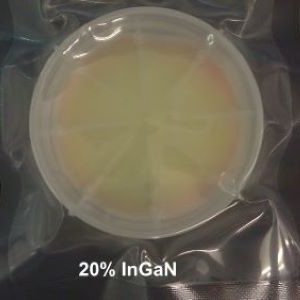
Undoped AlN Template on Sapphire, 2″, AlN layer 2um or 4um – single side polished or double side polished
Undoped AlN Template on Silicon, 2″, AlN layer 1um – single side polished
Undoped AlN Template on Sapphire, 4″, AlN layer1um – single side polished or double side polished
Undoped AlN Template on Silicon, 4″, AlN layer1um – single side polished (GANW190813-ALN)
2″ 25nm AlN on (111) Si
6″ 25nm AlN on (111) Si
Undoped AlN Template on 4″ Silicon ( Si <111>, P type, B-doped ) 4″x 500 nm
2. Specifications of AlN on Sapphire Substrate
2.1 2″ Size AlN-coated Sapphire Substrate
| Item | GANW-AlNT-SI |
| Diameter | 50.8mm ± 1mm |
| AlN Thickness: | 2um or 4um |
| Conduction Type | Semi-Insulating |
| Orientation | C-axis(0001)+/-1° |
| Orientation Flat | A-plane |
| XRD FWHM of (0002) | <150 arcsec. |
| XRD FWHM of (10-12) | <450 arcsec. |
| Structure | 1-5um AlN/AlN buffer/Sapphire |
| Substrate: | sapphire,430+/-25um |
| Edge Exclusion | ≤2.5mm |
| Through Crack | None |
| Useable Surface Area | ≥90% |
| Surface | Single side polished, Epi-ready |
| Packing: under nitrogen atmosphere, in a 100 clean room environment. | |
2.2 4″ Size AlN on Sapphire Wafer Substrate
| Item | GANW-AlNT-S 190822 |
| Diameter | Dia.100mm ± 1mm |
| Conduction Type | Semi-insulating |
| Thickness: | 1um |
| Substrate: | Sapphire |
| Orientation : | C-axis(0001)+/-1° |
| Orientation Flat | A-plane |
| XRD FWHM of (0002) | <1000 arcsec. |
| Surface Roughness | <2nm |
| Useable Surface Area | ≥90% |
| Polish Condition | Single side polished or double side polished. |
| Package | Single wafer container, under a nitrogen atmosphere, in a class 100 clean room environment. |
3. Epitaxial Growth of AlN on Sapphire
So far, because of its high transparency and cost-effective in the UV region, sapphire substrate is still the first choice for AlN heteroepitaxial. However, AlN/sapphire lattice mismatch and thermal expansion coefficient mismatch are seriously, so the AlN on sapphire dislocation density, especially the threading dislocation density (TDD), is great challenge for us to overcome.
Many technologies have been proposed and great progress has been made in reducing the TDD of AlN on sapphire growth, such as (MOCVD) and migration-enhanced MOCVD (MEMOCVD). In addition, the epitaxial lateral overgrowth (ELO) technology on micro-stripe patterned sapphire or AlN/sapphire template has also attracted widespread attention, which has significantly reduced TDD.
4. Template of AlN on Silicon by Coating
4-1 2″ 25nm AlN on (111) Si
4-2 6″ 25nm AlN on (111) Si
4-3 Undoped AlN Template on 2″ Silicon ( Si <111> N type ) 2″x 500 nm
4-4 Detail Specification of AlN Template on Silicon
Nominal AlN thickness: 500nm ±10%, one side coated, undoped AlN film
Back surface: silicon N-type
AlN orientation: C-plane (0001)
Wafer base: Silicon [111] N type, 2″ dia x 0.5 mm, one side polished
Undoped AlN Template on 4″ Silicon ( Si <111>, P type, B-doped ) 4″x 500 nm
Please Note:
For AlN-on-Silicon template, Ganwafer currently possesses two ways: one way is to grow AlN on silicon by MOCVD; another way is to coat AlN thin film on silicon substrate. Anyway, the AlN thickness should be around 200nm. If too thick the epitaxial layer, the BOW would be big. When epitaxial growth of AlN/Silicon wafer, it is better to choose silicon (111) substrate wafer since the resistivity will be higher.