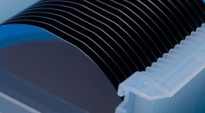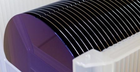
InSb MBE Growth
Indium antimonide (InSb), as a III-V binary compound semiconductor material, has stable physical and chemical properties and excellent process compatibility. InSb has a very narrow band gap, a very small electron effective mass and a very high electron mobility. It is particularly noteworthy that InSb belongs to intrinsic absorption and has a quantum efficiency of nearly 100% within the spectral range of 3~5um, making it the preferred material for preparing mid wave infrared detectors. It has enormous application prospects and commercial demand. The use of MBE growth to epitaxial InSb, InAlSb, InAsSb and other thin films on InSb substrates not only allows the preparation of PIN structures or other more complex structures, but also allows a certain proportion of in situ doping of the material during the growth process to improve the overall performance of devices.
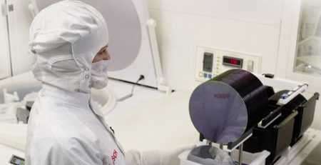
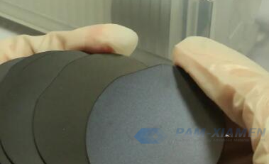
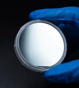
Ganwafer can provide MBE growth service of InSb epi-wafer with customized design for your researches. Take the epi structure for your reference:
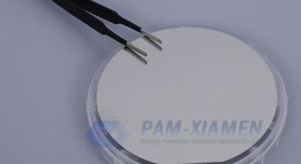
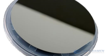
1. 2″ InSb Epitaxial Wafer by MBE Growth
|
2inch InSb based MBE Epilayer Growth (GANW210420 – INSBE) |
||||
| Layer No. | Material | Dopant | Doping Concentration | Thickness |
| 7 | P+-type InSb | Be | – | – |
| 6 | P-type InSb | – | – | |
| 5 | P-type InAlSb | – | – | – |
| 4 | i InSb | nid | – | – |
| 3 | N+type InSb | – | – | – |
| 2 | N+type InAsSb | – | – | 1um |
| 1 | N+-type InSb buffer | – | 1×1018 cm-3 | – |
| N-type InSb substrate | ||||
2. About InSb Molecular Beam Epitaxy Process
The main influencing factors of MBE InSb growth are temperature, V/III beam current ratio, etc.
Growth temperature is one of the most important factors affecting the crystal quality of molecular beam epitaxial materials. Temperature affects the adhesion coefficient, growth rate, background impurity density, doping situation, surface morphology, and interfaces between different epitaxial layers of various elements. When the substrate temperature is too high, it is easy to cause deviation in the chemical ratio of the epitaxial film, causing In precipitation and the formation of defects. In addition, it also affects the electrical properties of the epitaxial film; When the growth temperature is too low, it leads to a deterioration of the surface layer morphology, and the epitaxial film surface is prone to the formation of Hill ock defects (hill shaped defects), which are observed under a microscope as orange peel like.
Therefore, optimizing the growth temperature is one of the key steps in the development of InSb epitaxial technology. There is a literature report that using a InSb substrate with (001) orientation off 2 °~3° towards (111) B can not only reduce the growth temperature but also prevent the formation of Hill ock defects, resulting in a well formed InSb epitaxial film with better electrical properties.
In addition, the beam ratio of V/III group elements is crucial, and different beam ratios have a significant impact on surface morphology of InSb MBE growth. Due to the different adhesion coefficients and migration rates of Sb and In atoms on the substrate surface, it affects the atomic arrangement on the InSb surface, thereby affecting the surface atomic restructuring and ultimately affecting the nucleation of the epitaxial film.
Thus, in order to obtain high-quality epitaxial films, it is necessary to choose an optimized V/III beam ratio. Monitor the surface atomic restructuring of InSb epitaxial films under different beam ratios through RHEED, and optimize the beam ratio range through the quality of epitaxial films after epitaxy. After multiple experiments, the optimized beam ratio obtained is around 2-3 times.
For more information, please contact us email at sales@ganwafer.com and tech@ganwafer.com.