Connection and Distinction among Wafer, Die, and Chip
We often receive the demands for “wafer”, “die”, and “chip” from customers. Among them, what Ganwafer can offer is the semiconductor wafer. So what is wafer, and what’s the difference of wafer, die and chip? Let’s make an explanation on these terms.
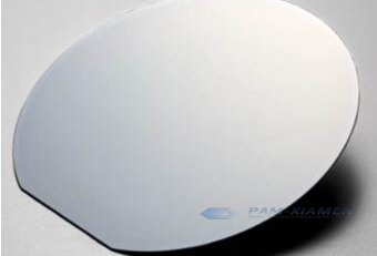
1. Wafer
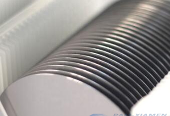
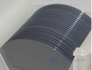
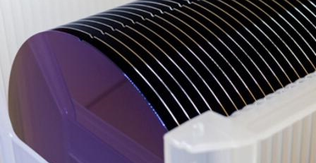
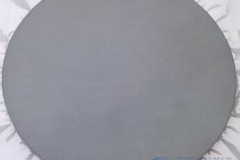
Wafer refers to the semiconductor wafer used in the manufacture of semiconductor integrated circuits. Because of its circular shape, it is called a wafer. Taking silicon wafer as an example, it is composed of pure silicon (Si) and is generally produced in 6 inches, 8 inches and 12 inches. It can be processed into various circuit element structures on the silicon wafer to become integrated circuit products with specific electrical functions.
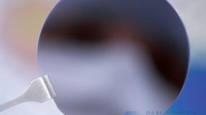
2. Die (Bare Wafer)
After photolithography and impurities are added, lattice-shaped grains are formed on the wafer, and the grains are called die. Grains are small crystals with irregular shapes that make up polycrystals, and each grain is sometimes composed of several sub-grains with slightly different orientations. The average diameter of the grains is usually in the range of 0.015~0.25mm, while the average diameter of the subgrains is usually on the order of 0.001mm. Generally speaking, each chip has a large number of dies.
The die is further divided into multiple cells, that is, functional units, such as IO units, power management units, etc. Cells are interpreted as “units” in integrated circuits, which are even smaller than die, and usually have such a relationship: wafer > die > cell.
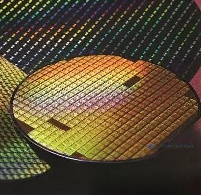
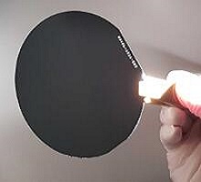
Die Formed on Wafer
3. Chip
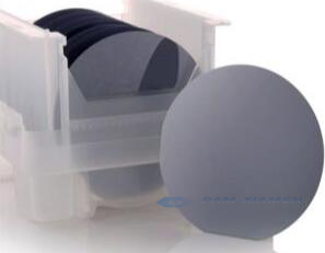
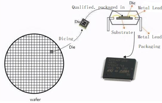
The wafer is first cut and then tested. The intact, stable, and full-capacity die is removed and packaged to form a chip that is seen in daily life. Generally, a chip is to use it as a carrier, and an integrated circuit is a result of many complicated design processes.
Cut out the qualified die for packaging, as shown in the figure:
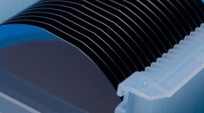
After the qualified die is cut, the original wafer will look like the picture below. Residual die are wafers of substandard quality. The black part is the qualified die, which will be packaged by the original factory and made into finished pellets, and the unqualified part, that is, the part left in the picture, will be treated as waste.
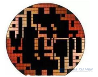
Unqualified Die on Wafer
For more information, please contact us email at sales@ganwafer.com and tech@ganwafer.com.