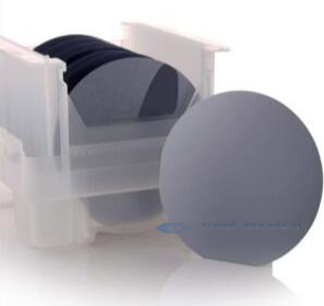
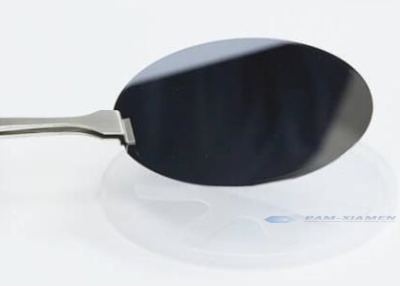
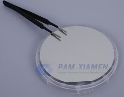
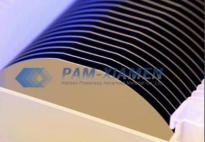
High Purity Undoped Single Crystal 4H-SiC Wafer
GaN/SiC HEMT microwave devices is suitable for new energy vehicles. In order to overcome the signal loss caused by parasitic capacitance related to the...
GaN/SiC HEMT microwave devices is suitable for new energy vehicles. In order to overcome the signal loss caused by parasitic capacitance related to the...
Indium antimonide (InSb) is III-V compound semiconductor material with extremely narrow band gap, extremely small electron effective mass and extremely high electron mobility. Due...
Group III-V compounds, especially gallium arsenide (GaAs), indium phosphide (InP), etc., are direct band gap materials. The top of the valence band and the...
808nm, 980nm or 9XXnm GaAs (gallium arsenide) epi wafer is used in edge emitting laser (EEL) for industrial welding, photolithography, medical applications, distance measurement...
Ganwafer, as a manufacturer focusing on the research and development, production and sales of compound semiconductor epitaxial stack wafers, includes InP and GaAs-based optoelectronic...
The parameters of silicon carbide epitaxial growth we are talking about actually depend mainly on the design of the device. For example, depending on...

Ganwafer can offer 650V GaN FETs Chip for fast charge products for the consumer market. GaN FETs advantages in the charger are mainly reflected...