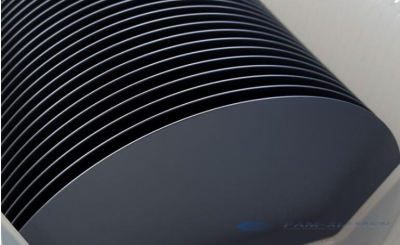
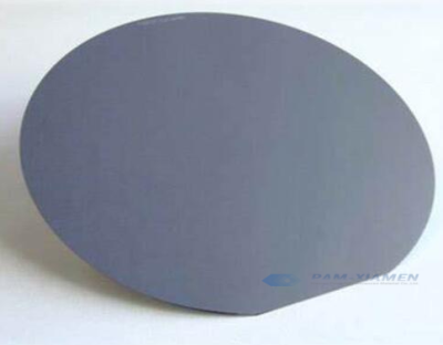
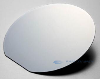
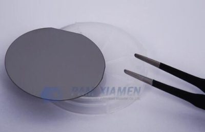
AlGaAs / GaAs Heterostructure
AlGaAs / GaAs heterostructure can be offered by Ganwafer. Aluminum gallium arsenide (AlGaAs), as an important optoelectronic basic material, is widely used in high-speed...
AlGaAs / GaAs heterostructure can be offered by Ganwafer. Aluminum gallium arsenide (AlGaAs), as an important optoelectronic basic material, is widely used in high-speed...
Heteroepitaxial InSb thin film directly on semi-insulating GaAs substrate and other III-V wafers are available. Epilayers of InSb and InSb alloys have attracted great...
Ganwafer can offer GaSb epitaxial wafer with type II superlattice (T2SL) structure. T2SL is a III-V group 6.1Å Sb-based material composed of InAs (6.0583...
Currently, in the preparation of blue LEDs, gallium nitride (GaN) materials are usually grown by means of heteroepitaxy. In commercial GaN based LED, most...
GaInAsP / GaInP / AlGaInP laser diode structure materials grown on GaAs substrate with a narrow waveguide is for fabricating laser diodes emitting wavelength...
Light emitting diode (LED) structure with GaInP / AlInP epilayers can be offered by Ganwafer. The ternary InGaP and AlInP materials are lattice matched...
InP (Indium Phosphide) material system includes ternary and quaternary III-V semiconductor materials, such as InGaAs, InGaAsP, InAlGaAs and InAlAsP, which are lattice matched to...
Photocathode epitaxial wafer is based on GaAs substrate epitaxial growth of AlGaAs/GaAs/AlGaAs, which is an important material of the third-generation micro-optical intensifier. The detector...
III-V compound semiconductor laser diode structures have been developed for more than half a century and their wavelength coverage ranges from deep ultraviolet to...
In1-xGaxAsyP1-y (indium gallium arsenide phosphide) is an alloy material of GaAs, GaP, InAs or InP. The band gap of InGaAsP can change through adjusting...
Indium arsenide (InAs) wafer material has great potential for fabricating different devices since its high electron mobility, narrow bandgap, high carrier concentration, and lattice-matched...
Indium gallium arsenide (InGaAs) wafer is a ternary compound semiconductor, which is suitable for detector applications. The InGaAs is lattice matched to InP substrate,...