Homoepitaxia de InAs sin dopar de tipo N en sustrato de InAs (001)
Arseniuro de indio (InAs) wafer material has great potential for fabricating different devices since its high electron mobility, narrow bandgap, high carrier concentration, and lattice-matched systems (InAs, GaSb, AlSb, and their alloys) at 6.1 A˚. Homoepitaxial InAs layer with different doping concentration on InAs (001) substrate can be used to manufacture avalanche photodiodes and photodetectors. InAs thin films with highly n-type doped, lightly doped or undoped are usually deposited as layers of plasmon-cladding and waveguide-space, which are for interband cascade laser and mid IR quantum cascade to help extend the wavelength. Homoepitaxy of InAs (001) can be offered by Ganwafer as below:
1. Estructura homoepitaxial de InAs
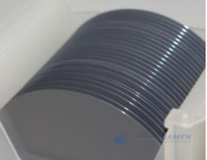
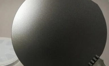
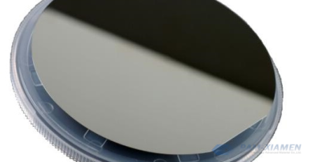
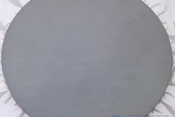
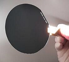
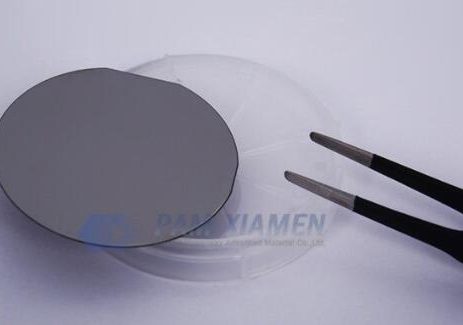
GANW200115-INAS
| Capa | Tipo/Dopante | Concentración de portadores (cm-3) | Espesor (um) |
| En Como(001) | tipo n/no dopado | <2x1016 cm-3 | 2-2.5 |
| InAs tipo n de 2 pulgadas (001), sustrato fuertemente dopado ((5-50)x1017 cm-3), parte trasera pulida | |||
La frecuencia de plasma de InAs altamente dopado es controlable en un amplio rango de frecuencias de infrarrojo medio, por lo que la homoepitaxia de InAs es ideal para la estructura de metamateriales y la plasmónica de IR medio. Con las amplias aplicaciones de la homoepitaxia de InAs (001), para facilitar el desarrollo de dispositivos de alto rendimiento, aumentan las demandas de epicapa de alta calidad con baja densidad de defectos y superficie atómicamente lisa. Es importante para dispositivos complicados, como láseres QC e IC.
2. Morfología de la superficie y densidades de defectos de la epicapa de homoepitaxia de InAs
Surface morphology and defect densities are important metrics that shows the quality of InAs thin film. The homoepitaxy InAs is highly doped with smooth surface that demonstrates the waveguide layer grown at high quality crystalline, contributing to sharp interfaces in the laser structure fabrication later. The structure is composed of untral thin layers up to 100 in interband / quantum cascade devices.
For InAs homoepitaxial growth, low defect density is critical since it can penetrate into the laser structure and become recombination center to degrade the performance of laser. Therefore, smooth surface morphology and low defect density are very important for realizing perfect performance of devices. To ensure the wafer quality, we can use SEM, AFM, and DIC microscopy to observe the homoepitaxial InAs layer after epitaxial growth process, and then optimize the conditions for growth of homoepitaxial InAs layer on InAs (001) substrate.
For more information, please contact us email at sales@ganwafer.com and tech@ganwafer.com.