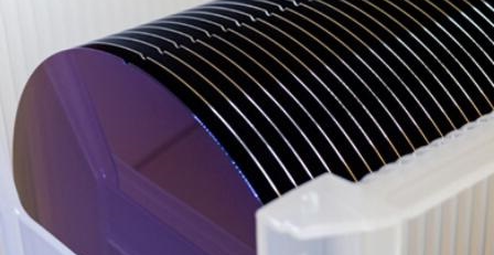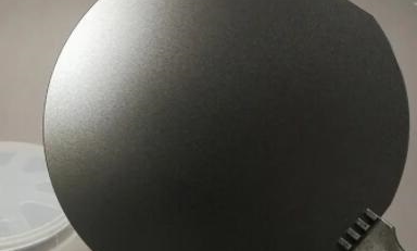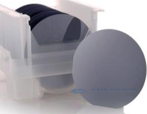
What is the Key Parameters of SiC Epitaxial Wafer?
The parameters of silicon carbide epitaxial growth we are talking about actually depend mainly on the design of the device. For example, depending on the voltage grade of the device, the parameters of the SiC epitaxial growth are also different.
1. SiC Epitaxy Key Parameters
Generally , the low pressure at 600 volts, the thickness of the silicon carbide epitaxy may be about 6 μm, and at medium pressure of 1200~1700, the thickness needed is 10~15 μm. For high voltages above 10,000 volts, 100 μm or more may be required. Therefore, with the increase of voltage capacity, the silicon carbide epitaxial growth thickness increases accordingly. Therefore, the high-quality epitaxial wafer preparation is very difficult, especially in the field of high voltage. The most important thing is defect control, which is actually a very big challenge.
2. Defects of Silicon Carbide Epitaxial Growth
Defects of silicon carbide epitaxial growth are generally divided into fatal defects and non-lethal defects:
Fatal defects, like triangular defects and drops, affect all device types, including diodes, MOSFET, bipolar devices. The biggest impact on the devices is breakdown voltage, which can reduce the breakdown voltage by 20%, or even drop to 90%.
Non-lethal defects, like some TSDs and TDs, may have no effect on the diode, but may have a life-span effect on MOS, bipolar devices, or some leakage effects, which will eventually affect the qualified processing rate of the device.
To control the defect of SiC epitaxy, the first method is to choose the silicon carbide substrate material carefully; the other is the equipment selection and localization, and the third is the process technology.
3. Progress in Silicon Carbide Epitaxial Growth Technology
In the field of low and medium pressure, the core parameter thickness and doping concentration of the SiC epitaxy can be achieved at a relatively excellent level.
However, in the field of high pressure, there are still many difficulties to overcome. The main parameter index includes thickness, uniformity of doping concentration, triangular defects and so on.
In the field of medium and low voltage applications, the silicon carbide epitaxial growth technology is relatively mature, and basically can meet the low-medium voltage SBD, JBS, MOS and other devices needs. As above a 1200-volt device application of 10μm epitaxial wafer, its thickness and doping concentration has reached a very excellent level, and the surface defect is also very good, can reach 0.5 square meters below.
The development of epitaxial technology in the field of high-voltage is relatively lagging behind. For example, the uniformity, thickness and concentration of a 200μm silicon carbide epitaxial material on 200 volts device compared to the above-mentioned in low pressure is quite different, especially the doping concentration uniformity.
At the same time, high-voltage devices need thick film. However, there still are many defects, especially triangular defects, in the SiC epitaxial wafers, which mainly affect the preparation of high-current devices. High currents require a large chip area, and the life expectancy is currently relatively low.
In terms of high voltage, the type of device tends to bipolar devices, the life requirements for minority carrier are relatively high. To achieve an ideal forward current, the minority carrier lifespan at least should reach more than 5μs, while the current minority carrier life time of SiC epitaxial wafer is about 1 to 2μs. Thereby, the demand for high-voltage devices is not yet met, and epitaxial growth of silicon carbide wafer still need post-processing technology.
For more information, please contact us email at sales@ganwafer.com and tech@ganwafer.com.