Silikon Gofretlerde İnce Film Biriktirme ve Metalizasyon

Ganwafer, a metal deposition manufacturing company, offers metal film deposition services on silicon by various metal thin film deposition techniques, such as evaporating, sputtering, LPCVD, ALD and etc. All the metal deposition on silicon wafer is supplied at different stress level with high thickness uniformity. The metal deposition process forms contacts in doped area between the semiconductor and conducting path. For our metal deposition service, we use metal and ITO (indium tin oxides) material to prepare electrodes for silicon substrate, and use non-metallic materials to grow sacrificial and insulating dielectric layers on silicon substrate.
- Description
- Inquiry
Description
During the metal deposition process, there are several requirements crucial for integrated microelectronic devices, which should be followed:
The purity of metal should be as high as enough;
It is possible to integrate stacked layers;
The current carrying capacity should be high;
The contact resistance between metal and semiconductor should be low;
The metalizing process should be simple;
The material for metallization should be corrosion-resistant and has a long life;
The material for deposition should be excellent adhesion on silicon oxides.
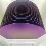
Take the following technical parameters of our deposition metal silicon wafer as an example:
1. Technical Parameters of Metal Deposition on Semiconductor
| 4″ Si Substrate + SiO2 + TiO2 + Pt | ||
| Item | Parameters | |
| Material | Monocrystalline Silicon | |
| Grade | Prime Grade | |
| Growth Method | CZ | |
| Diameter | 100.0±0.3mm, 4″ | 100 ±0.3mm, 4″ |
| Conductivity type | N type | N type |
| Dopant | Phosphorus | Un-Doped |
| Orientation | <100>±0.5° | [111]±0.5° |
| Thickness | 300±25μm (Total Thickness) | 525±25μm |
| Resistivity | 1-10Ωcm | n/a |
| Primary Flat | SEMI STD Flats | SEMI STD Flats |
| Secondary Flat | SEMI STD Flats | SEMI STD Flats |
| Surface Finish | One Side Polished | |
| Edge Rounded | Edge Rounded Per SEMI Standard | |
| Si Sub/SiO2/TiO2/Pt | Total Thickness 300μm Si Substrate Thickness 289μm 1st Middle Layer SiO2 Thickness 10,000 Angstrom 2nd Middle Layer Ti Thickness 500 Angstrom Top Layer Pt 5000 Angstrom |
Si Substrate Thickness 525μm 1st Middle Layer SiO2 Thickness 300 Angstrom 2nd Middle Layer Ti Thickness 20 Angstrom Top Layer Pt Angstrom |
| Particle | SEMI STD | |
| TTV | <10um | |
| Bow/Warp | <30um | |
| TIR | <5µm | |
| Oxygen Content | <2E16/cm3 | |
| Carbon Content | <2E16/cm3 | |
| OISF | <50/cm² | |
| STIR (15x15mm) | <1.5µm | |
| MCC Lifetime | N/A | |
| Surface Metal Contamination Fe,Zn, Cu,Ni, K,Cr |
≤5E10 atoms/cm2 | |
| Dislocation Density | SEMI STD | |
| Chips, scratches, bumps, haze, touch marks, orange peel, pits, cracks, dirt, contamination | All None | |
| Laser Mark | SEMI STD | |
2. Metal Deposition Techniques
2.1 Atmospheric Pressure CVD (APCVD)
APCVD is one of CVD methods for doped or undoped oxides deposition. Due to the low temperature in the process, a low density and a moderate coverage of deposited oxide will be obtained. The high output of the metal deposition substrate is great advantage of APCVD process.
2.2 Low Pressure CVD (LPCVD)
In the LPCVD method, vacuum is used. Silicon nitride (Si3N4), silicon oxynitride (SiON), silicon dioxide (SiO2) and tungsten thin film can be deposited on silicon substrate by this method, obtaining the metallized wafer with high conformity.
2.3 Atomic Layer Deposition (ALD)
ALD is a CVD process improved suitable for depositing metallic thin films on Si substrate. Using ALD can deposit 3D structures very uniformly. Both insulating and conductive films can be grown on different substrates (semiconductors, polymers, etc.).