KENDİNİZİ OLUŞTURUN YARI İLETKEN WAFER
Ganwafer possesses a strong technical R&D team, constantly improving the quality of existing wafers, like SiC, GaN and III-V compound, and developing latest material and devices as per the market.

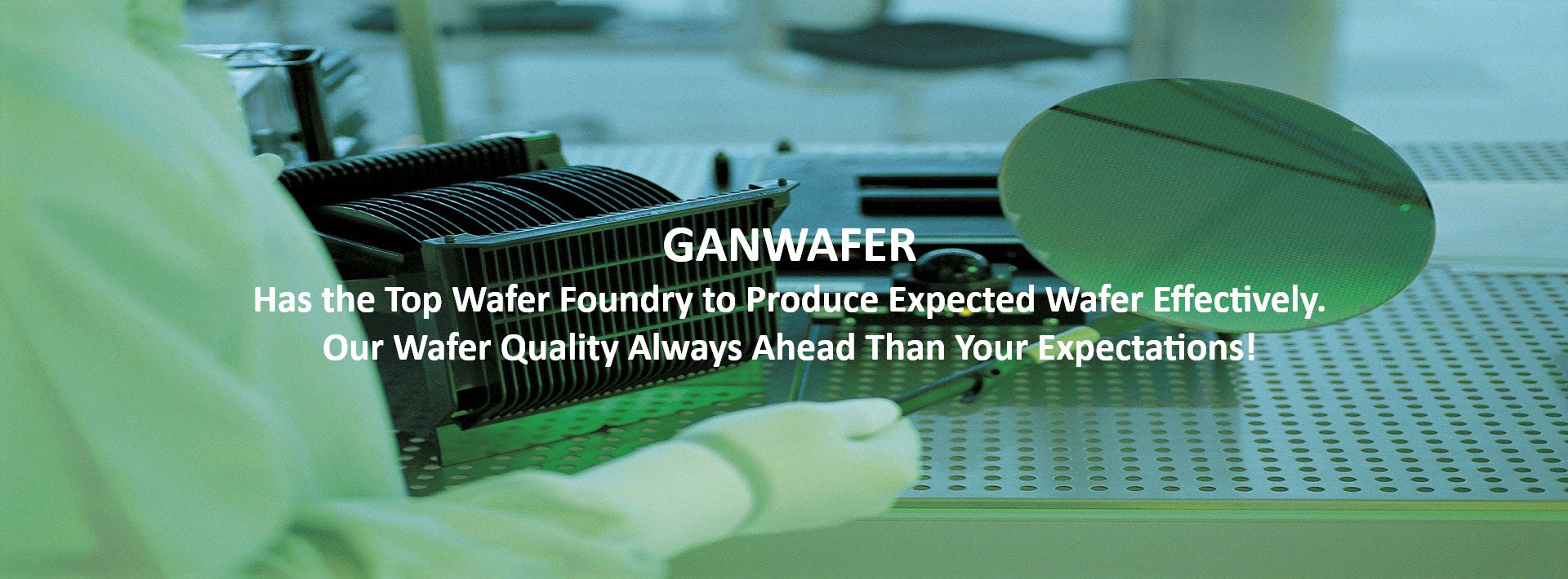
Semiconductor Wafer Technology At Ganwafer
As a condensed matter physics research center and a leading manufacturer of compound semiconductor material in China, Ganwafer, we specialize in creating cutting-edge crystal growth and epitaxy technologies.
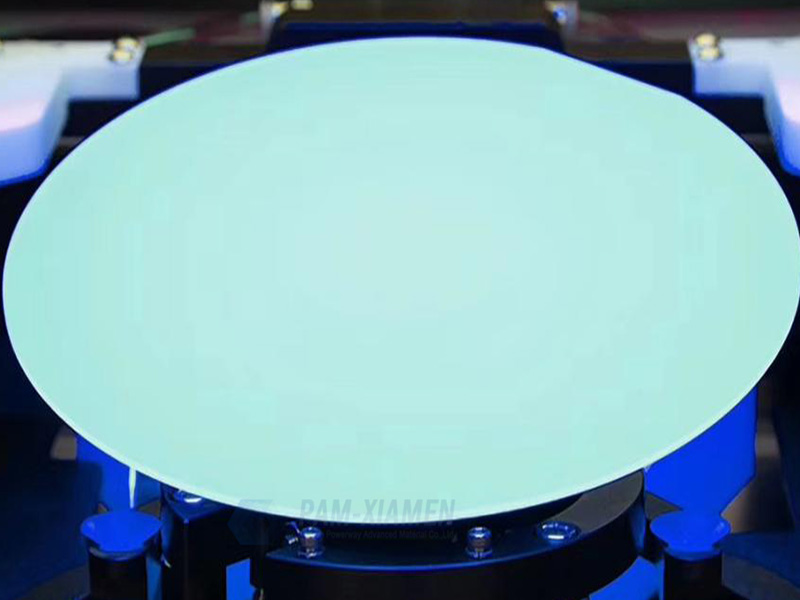
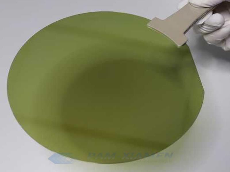
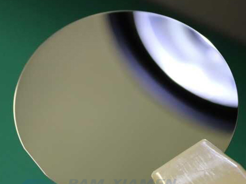
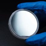
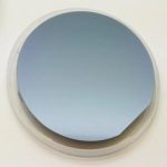
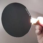
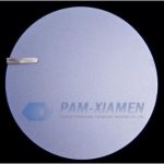
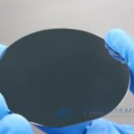
Bir gofret, özellikle yüksek güçlü cihaz veya RF cihazı üretmek için entegre devrelerin imalatında kullanılan SiC veya GaN Wafer gibi bir yarı iletkenin ince bir dilimini temsil eder.
Gofret Kategorimiz
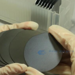
Önde gelen bir araştırma ve üretim şirketi olarak, 1990'dan beri CZ silikon gofret ve külçe araştırma ve yaratmaya ve ardından 2004'ten beri ikinci nesil GaAs ve InP gofret ve üçüncü nesil SiC ve GaN gofret geliştirmeye kendimizi adadık. substrat ve epitaksi dahil gofret, III-V gofret ve silikon gofret.
Son Haberler
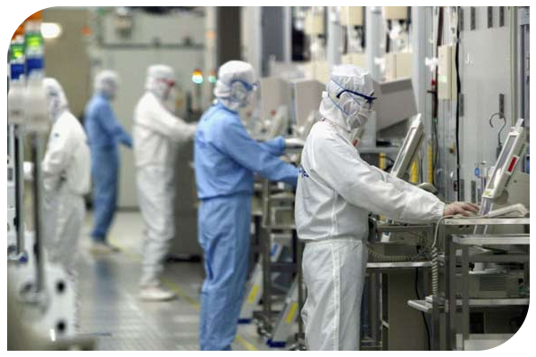
Neden bizi seçmelisiniz

In order to get the most efficient services, you need to hire a professional and highly skilled compound semiconductor material manufacturing company. This is where Ganwafer plays a significant role that concentrates on superior systems, unconventional engineering design, and practical research.
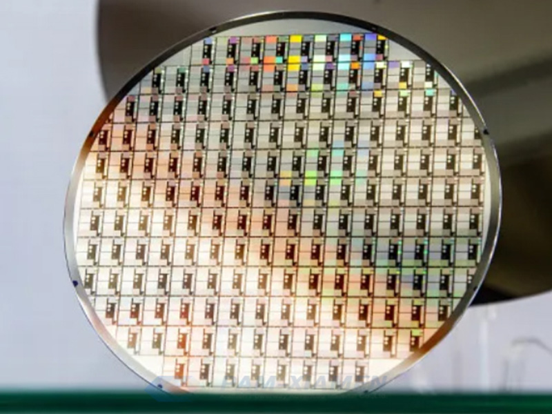
Yarı iletken gofretlerin, en sık kullanılan elektronik cihazlarımızın üretim prosedürünün en önemli parçası olduğunu bilmelisiniz. Çeşitli elektronik cihazların devrelerinin sorunsuz çalışmasına yardımcı olur ve verim oranını etkiler. Bilgi ve teknoloji yoğun bir kuruluş olarak, bileşik yarı iletken gofretlerin araştırma ve üretiminde uzmanız. Yarı iletken kristal büyümesini, süreç geliştirmeyi ve epitaksiyi entegre eden bileşik yarı iletken malzeme sunuyoruz. Yüksek kaliteli, ustalıkla üretilmiş gofret ürünleri arıyorsanız, evinizden bir telefon kadar uzağınızdayız. Tereddüt etmeden bugün bizi arayın.
Bize Ulaşın
Ganwafer is a top-class enterprise for compound semiconductor material integrating semiconductor crystal growth, process development, and epitaxy.