Photo Mask
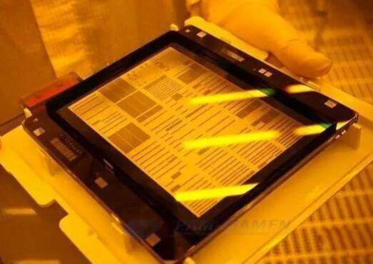
Semiconductor photomask is a film based on photolithography process. The photomask in semiconductor is a graphic transfer tool or master in the microelectronics manufacturing process, and it is a carrier of intellectual property information such as graphic design and process technology. Semiconductor photomask can be classified into chromium plates, dry plates, liquid relief plates and film according to their uses.
The photomask manufacturing process is as follows: According to the pattern required by the customer, we one of leading semiconductor photomask manufacturers use the photolithography process to engrave micron and nano-level fine patterns on the mask. The raw material of the mask is a photosensitive photomask blanks for making fine photomask patterns, and then the unnecessary metal layer and glue layer are washed away to obtain the semiconductor masking plate.
- Description
- Inquiry
Description
Photomasks can be divided into quartz masks, soda masks and others (including relief plates and film) according to different substrate materials. Specifically as follows:
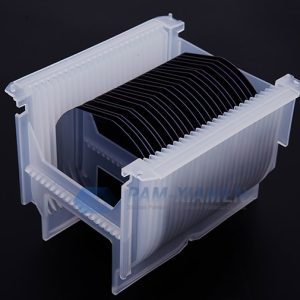
Quartz photomask semiconductor uses quartz glass as the substrate material, which has high optical transmittance and low thermal expansion rate. Compared with soda glass, it is more flat and wear-resistant and has a long service life. Quartz photomask is mainly used for high-precision masks;
The soda mask uses soda glass as the substrate material, which has higher optical transmittance, relatively higher thermal expansion rate than quartz glass, and relatively weaker flatness and wear resistance than quartz glass. It is mainly used for medium and low precision masks;
The relief photomask design use with unsaturated polybutadiene resin as the substrate material, which is mainly used for oriented material pad printing in the manufacturing process of liquid crystal displays (LCD);
The semiconductor mask design uses PET as the substrate material, which is mainly applied for circuit board masks.
1. Semiconductor Photomask Solutions
1.1 Photomask on Quartz Substrate
| Customer Information Confirmation Form | ||
| 1 | Customer name | — |
| 2 | Mask size | 5009 |
| 3 | CD SPEC(On mask) | — |
| 4 | Mask Scale | 5:01 |
| 5 | Mask Grade | S |
| 6 | Mask Material | Quartz |
| 7 | Pellicle | None |
| 8 | Pellicle type | I-Line |
| 9 | Data sending | FTP |
| 10 | JDV(Jobview check) | YES |
| 11 | Lithography machine type | — |
| 12 | CD (CD match) | YES |
| 13 | Registration match | YES |
| 14 | Defect Inspection | Die to Die/Die to Database |
| 15 | Allow Scratch within 5mm on the edge of | YES |
| the mask but out of the data | ||
| 16 | Special request | — |
Grades for Photomask on Quartz
| Grade | D | C | B | A | S |
| Tolerance | ±0.3 | ±0.3 | ±0.2 | ±0.15 | ±0.1 |
| Mean to target | ±0.3 | ±0.3 | ±0.2 | ±0.15 | ±0.1 |
| Uniformity | 0.2 | 0.2 | 0.2 | 0.15 | 0.1 |
| Registration | ±0.4 | ±0.3 | ±0.2 | ±0.15 | ±0.1 |
| Defect size | 1.5 | 1.5 | 1 | 0.8 | 0.6 |
| Defect density | 0 | 0 | 0 | 0 | 0 |
1.2 1X Master Semiconductor Photomask on Quartz or Soda Lime
| Product | Dimensions | Substrate Materials |
| 1X Master | 4” X4” X0.060” or 0.090” | Quartz and Soda Lime |
| 5” X5” X0.090” | Quartz and Soda Lime | |
| 6” X6” X0.120” or 0.250” | Quartz and Soda Lime | |
| 7” X7” X0.120” or 0.150” | Quartz and Soda Lime | |
| 7.25” Round X 0.150” | Quartz | |
| 9”X9”X0.120” or 0.190” | Quartz and Soda Lime |
1.2.1 Common Specifications for 1X Master Masks (Quartz Material)
| CD Size | CD Mean-to-Nominal | CD Uniformity | Registration | defect Size |
| 2.0 um | ≤0.25 um | ≤0.25 um | ≤0.25 um | ≥2.0 um |
| 4.0 um | ≤0.30 um | ≤0.30 um | ≤0.30 um | ≥3.5 um |
1.2.2 Common Specification for 1X Master Masks (Soda Lime Material)
| CD Size | CD Mean-to-Nominal | CD Uniformity | Registration | defect Size |
| ≤4 um | ≤0.25 um | ———— | ≤0.25 um | ≥3.0 um |
| ≤4 um | ≤0.30 um | ———— | ≤0.45 um | ≥5.0 um |
1.3 UT1X Mask Dimensions and Substrate Materials
| Product | Dimensions | Substrate Material |
| UT1X | 3″ X5″ X0.090″ | Quartz |
| 5″ X5″ X0.090″ | Quartz | |
| 6″ X6″X0.120″ or 0.250″ | Quartz |
Common Specifications for UT1X Masks
| CD Size | CD Mean-to-Nominal | CD Uniformity | Registration | defect Size |
| 1.5 um | ≤0.15 um | ≤0.15 um | ≤0.15 um | ≥0.50 um |
| 3.0 um | ≤0.20 um | ≤0.20 um | ≤0.20 um | ≥0.60 um |
| 4.0 um | ≤0.25 um | ≤0.25 um | ≤0.20 um | ≥0.75 um |
1.4 Standard Binary Mask
| Product | Dimensions | Substrate Materials |
| 2X | 6″X 6″ X0.250″ | Quartz |
| 2.5X | ||
| 4X | ||
| 5X | 5″ X5″ X0.090″ | Quartz |
| 6″ X6″ X0.250″ | Quartz |
Common Specifications for Standard Binary Masks
| CD Size | CD Mean-to-Nominal | CD Uniformity | Registration | defect Size |
| 2.0 um | ≤0.10 um | ≤0.15 um | ≤0.10 um | ≥0.50 um |
| 3.0 um | ≤0.15 um | ≤0.15 um | ≤0.15 um | ≥0.75 um |
| 4.0 um | ≤0.20 um | ≤0.20 um | ≤0.20 um | ≥1.00 um |
1.5 Medium Area Masks
| Product | Dimensions | Substrate Materials |
| 1X | 9″ X9″ 0.120″ | Quartz Soda Lime(both Chrome and Iron Oxide absorbers available) |
| 9″ X9″ 0.190″ | Quartz |
1.5.1 Common Specifications for Medium Area Masks (Quartz Material)
| CD Size | CD Mean-to-Nominal | CD Uniformity | Registration | defect Size |
| 0.50 um | ≤0.20 um | ———— | ≤0.15 um | ≥1.50 um |
1.5.2 Common Specifications for Medium Area Masks (Soda Lime Material)
| CD Size | CD Mean-to-Nominal | CD Uniformity | Registration | defect Size |
| 10 um | ≤4.0 um | ———— | ≤4.0 um | ≥10 um |
| 4 um | ≤2.0 um | ———— | ≤1.0 um | ≥5 um |
| 2.5 um | ≤0.5 um | ———— | ≤0.75 um | ≥3 um |


