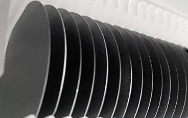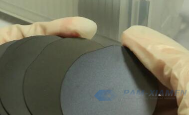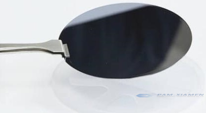
InSb Epitaxial Layer on GaAs
Heteroepitaxial InSb thin film directly on semi-insulating GaAs substrate and other III-V wafers are available. Epilayers of InSb and InSb alloys have attracted great attention because of their potential in infrared optoelectronic devices. There are several epitaxy techniques for epitaxial layer growth of InSb, such as MBE, MOCVD, MSE and LPE. The InSb epitaxial layer also can be grown on Si, InP and other substates. More info about our InSb semiconductor epitaxial layer grown on undoped GaAs substrate, please refer to the following part:
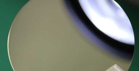
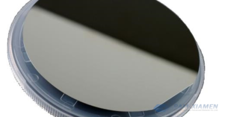
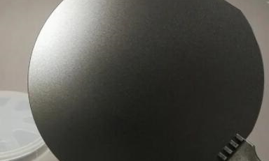
1. InSb Epitaxy on GaAs Substrate
GANW200810- INSB
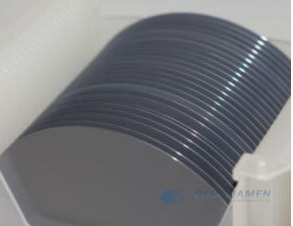
Epi layer: 3um, undoped InSb
Substrate: 2“size, undoped GaAs
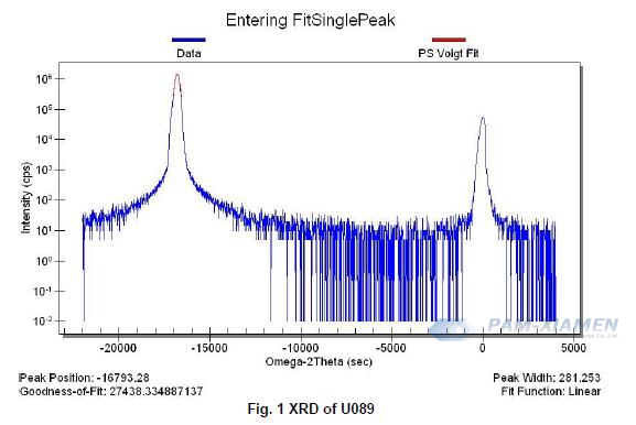
Following is the XRD diagram of GaAs based InSb eptaxial crystal wafer:
Remarks:
1/ For InSb epi layer semiconductor, generally, the higher the doping concentration, the stronger the absorption;
2/ If the wavelength (photon energy) of the laser is larger than the forbidden band width of indium antimonide, it will be completely absorbed. The wavelength of the laser is relatively short (the photon energy is larger than the band gap of InSb);
3/ In terms of non-doped InSb (undoped InSb or semi-insulating InSb), it has a concentration of < 9E14.
2. How to Improve Quality of InSb Epitaxial Layer on GaAs ?
In terms of photodetector applications, epitaxial growth of InSb films on GaAs substrates or Si substrates is beneficial to monolithic integration of large-area InSb detector arrays with GaAs-based or Si-based signal readout and processing components. However, there is a large degree of lattice mismatch (14.6%) between the heteroepitaxial InSb film and the GaAs substrate. The GaAs substrate material has semi-insulating and high-resistance properties, so when studying the Hall electrical properties of InSb epitaxial thin film materials, the GaAs substrate is usually used for the heteroepitaxial growth of InSb, and then the four-probe method is used to measure InSb layer characterization – electrical properties by the four-probe method on a Hall tester
Due to the high density of dislocations at the interface caused by the lattice mismatch, a large number of defects, like threading dislocations (TDs), microtwins (MTs), and cracks located around interfaces, are generated in the InSb epi layer, which affects the film quality and device performance. Therefore, reducing the defect density of InSb epi on GaAs is crucial for practical applications.
Currently, some growth techniques are suggested to minimize the defects caused by lattice mismatch. For example, metamorphic buffering techniques have been developed on GaAs substrate. According to several reports on the growth of high-quality InSb on GaAs substrates, the lattice mismatch problem can be partially solved by using AlSb and InAlSb’s graded buffer (SGB). It is also important to provide optimal growth conditions, such as growth temperature and growth rate, for AlSb and InAlSb SGB. In addition, In1-xAlxSb/In1-yAlySb short-period superlattice work can be used to reduce dislocation of InSb epitaxial layer by changing the composition of In and Al.
For more information, please contact us email at sales@ganwafer.com and tech@ganwafer.com.