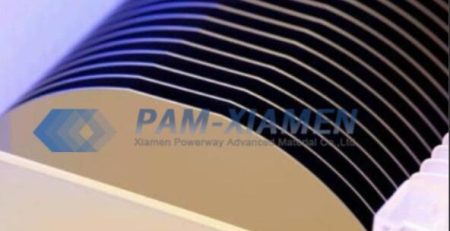
GaInP / AlGaInP LED Structure Grown on GaAs Substrate
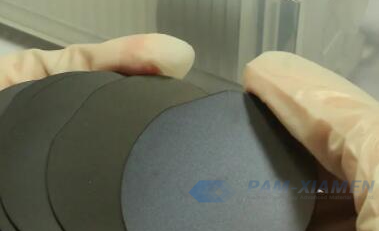
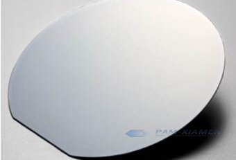
Ganwafer can supply GaAs based LED wafer with GaInP / AlGaInP multi-quantum wells (MQWs). There are two categories of LEDs used in the lighting field, one is an alloy of aluminum phosphide, gallium phosphide and indium phosphide (AlGaInP or AlInGaP), which can be made into red, orange and yellow LEDs; the other is indium nitride alloys with gallium nitride (InGaN) can be made into green, blue and white LEDs. Most of the luminescent materials are III-V group. At present, light-emitting diodes use materials with direct band gaps. The emission wavelength of AlGaInP / GaInP / GaAs visible light emitting diode covers the visible light band of 570-690 nm and the color is from yellow-green to dark red. Dark red LEDs with special wavelengths of 670 and 680 nm can be used in the fields of movie reproduction, medical treatment, and crop growth. Take the AlGaInP LED wafer for example:
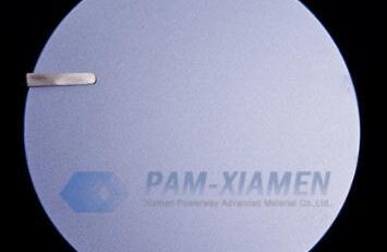
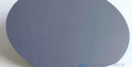
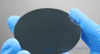
1. GaAs based AlGaInP LED Wafer Structure
GANWP20162-LED
| Layer | Composition | Dopant | Concentration | Thickness (nm) |
| Top contact | p-GaAs | C | – | – |
| Spreader | p-Al0.45Ga0.55As | C | – | – |
| Cladding | p-Al0.5In0.5P | Zn | – | |
| Barrier | Al0.25Ga0.25In0. 5P | – | – | |
| 4 x well | In0.56Ga0.44P | – | – | |
| 4 x barrier | Al0.25Ga0.25In0. 5P | undoped | – | |
| Cladding | n-Al0.5In0.5P | Si | – | – |
| Spreader | n-Al0.45Ga0.55As | Si | – | 800 |
| Bottom contact | n-GaAs | Si | – | – |
| Al0.5In0.5P | – | – | ||
| Buffer | GaAs | – | – | |
| Substrate | GaAs |
Note:
# The PL wavelength of AlGaInP LED wafer for sale would be around 671nm with a tolerance of +-10nm or so;
# Regarding the surface requirement, it should be visually shiny (like polished);
# Surfscan: defects @ > 6.0 microns should be < 20 cm-2;
# The lattice quality of GaAs buffer is better than that of the substrate, which can eliminate the influence of the substrate on epitaxy.
2. Why Used AlGaInP / GaInP MQWs to Grow LED Epitaxy?
The AIGaInP / GaInP semiconductor material has a suitable band gap and the lattice is matched with GaAs substrate. During the AlGaInP LED wafer manufacturing process, due to the strong energy of oxygen and aluminum, when the composition of aluminum becomes larger, the content of residual deep-level impurity oxygen in the active region increases, resulting in enhanced non-radiative recombination. In addition, the use of multiple quantum well (MQW) materials in AlGaInP LED wafer technology has the following advantages. On one hand, due to sub-effects, the use of smaller aluminum components can also obtain shorter wavelengths; on the other hand, in the quantum well, there is higher radiation efficiency. Therefore, the GalnP / (AlxGa1-x)InP multiple quantum wells are ideal for the production of high-brightness light-emitting diodes (LEDs).
For more information, please contact us email at sales@ganwafer.com and tech@ganwafer.com.