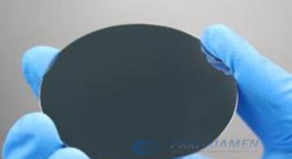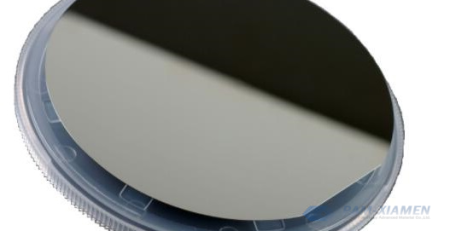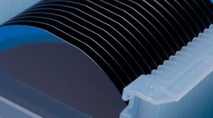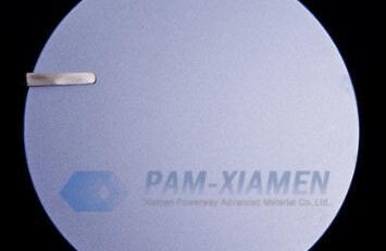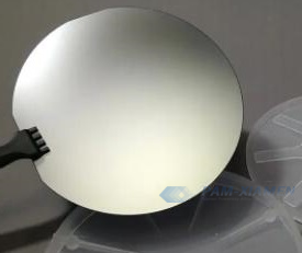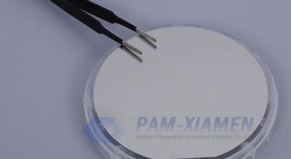
GaAs Photocathode Epitaxial Wafer
Photocathode epitaxial wafer is based on GaAs substrate epitaxial growth of AlGaAs/GaAs/AlGaAs, which is an important material of the third-generation micro-optical intensifier. The detector unit made of GaAs photocathode wafer can quickly respond to near-infrared light, and is widely used in the field of low-light night vision. III-V epi wafer for photocathode material provided by Ganwafer is grown on GaAs substrate with protective films.
1. Specification of GaAs Epitaxial Wafer for Photocathode
1.1 GaAs-Photocathode Structure with Buffer Layer AlxGa1-xAs
1.2 GaAs Photocathode Epitaxial Heterostructure
| 50mm GaAs Photocathode Epi-Wafer with Protective Layers (GANW200311-GAAS) | |||
| Epi Layer | Material | Carrier Concentration | Thickness |
| 1 | water-soluble protective layer | – | 1 um |
| 2 | SiO | – | – |
| 3 | p-Al(0.6)Ga(0.4)As:Zn | – | – |
| 4 | p+ – GaAs:Zn | – | – |
| 5 | p-Al(0.6)Ga(0.4)As:Zn | – | – |
| 6 | Wafer n-GaAs:Si | (1÷4)*1018 cm-3 | 500um |
| 7 | water-soluble protective layer | 1 um | |
| Note: a. Deviation of layer thickness is +/-10%;
b. The material of protective film is SiN passivation layer. |
|||
2. About GaAs Photocathode
The earliest and more mature group III-V semiconductor photocathode is photocathode based on GaAs substrate, and GaAs photocathode spectral response range is in the visible light region of 400-1000 nm, which is mainly used in the field of low-light detection. Since GaAs epitaxial photocathode has the characteristics of wide response band, there are problems such as large response noise and incapability of all-weather use in the application of narrow-band response fields such as ocean detection. Due to the limitations of the field, a GaAlAs photocathode with tunable Al composition is proposed to make it sensitive to blue-green light.
Photocathode fabricated on GaAs wafer is by far the most widely used photocathode in the field of low-light night vision. The GaAs photocathode quantum efficiency (QE) is high, and dark emission is low. In addition, there are many advantages. The energy distribution and angular distribution of the emitted electrons are concentrated, the long-wave valve is adjustable, and the long-wave response expansion potential is large.
3. GaAs Photocathode Activation
GaAs based photocathode epitaxial wafer is the primary choice for producing spin-polarized electron beam with high brightness, high polarization and fast polarization inversion. But due to the high reactivity of the emitting surface, it has very short lifetime, leading to difficulties in operation. Researchers use material, like Cs2Te, with more hardness to activate GaAs. This method shows a polarization comparable to the Cs-O activation and increase lifetime because of the the Cs2Te layer firmness.
It is reported that the photocathode QE based on Cs-Te activation on GaAs material is lower than that activated on Cs-O. In terms of Cs-Te activation, the QE of photocathode is 6.6% at wavelength of 532 nm, while the QE is about 8.8% and 4.5% at 532 nm and 780 nm respectively through Cs-O-Te activation. It is obviously seen that higher quantum efficiency and longer lifetime of negative electron affinity GaAs photocathode can be obtained by Cs-O-Te solution.
For more information, please contact us email at sales@ganwafer.com and tech@ganwafer.com.