Si-Delta Doped GaAs PHEMT Heterostructure
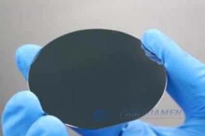
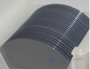
As a leading semiconductor wafer manufacturer, Ganwafer can supply III-V semiconductor epitaxial wafers, more specifications please refer to https://www.ganwafer.com/product/iii-v-epi-wafer/. Here we take the delta doped GaAs pHEMT (pseudo-matched high electron mobility transistor) heterostructure for example, and the specific layer materials of delta doped heterostructure DpHEMT with a stop layer are listed as the table below. PHEMT is one of the most widely used microwave and millimeter-wave power devices. In the double δ-doped GaAs pHEMT material structure, the interface characteristics and growth quality of the strained layer InGaAs channel are the keys to determine the performance of the material. It is found that double delta doping effectively increases the carrier concentration of the GaAs pHEMT compared with single delta doping.
1. Delta Doped pHEMT Heterostructure
1.1 Epitaxial pHEMT Structure on GaAs Substrate
GANW201028-PHEMT
| layer name |
|
Thickness, um |
conductivity type |
|
|
| contact layer | H17 | 0.080 | N | GaAs | 5.0×10¹⁸ |
| stop layer | H16 | – | – | Al0.9Ga0.1As | – |
| barrier layer | H15 | – | – | Al0.22Ga0.78As | – |
| spacer layer | H14 | – | – | GaAs | – |
| delta layer | H13 | – | – | Si | – |
| spacer layer | H12 | 0.0004 | – | GaAs | – |
| spacer layer | H11 | – | – | Al0.23Ga0.77As | – |
| spacer layer | H10 | – | – | GaAs | – |
| channel layer | H9 | – | – | In0.23Ga0.77As | |
| spacer layer | H8 | – | – | GaAs | – |
| spacer layer | H7 | – | – | Al0.23Ga0.77As | – |
| spacer layer | H6 | – | – | GaAs | – |
| delta layer | H5 | – | – | Si | 0.74×10¹² CM-2 |
| spacer layer | H4 | 0.0004 | – | GaAs | – |
| barrier layer | H3 | – | – | Al0.23Ga0.77As | – |
| buffer heterostructure |
H2 |
– | – | GaAs,AlGaAs | – |
| substrate
(001) |
H1 |
625±25 | – | GaAs | – |
1.2 Specification of Epitaxial РНЕМТ–1δ Structure on GaAs Substrate for Low Noise MMIC Applications
GANW190213-PHEMT
| Layer Material | Thickness | Doping (Concentration) | Notes |
| N+ GaAs | — | Si doped,(6E18 cm-3) | |
| n-AlxGa1-xAs | — | Si doped, (–) | X=0.24±0.005 |
| i-AlxGa1-xAs | 7 | Undoped | X=0.24±0.005 |
| Delta- Si | — | Planar Si doped, (–) | |
| i-GaAs | — | Undoped | |
| i-AlxGa1-xAs | — | Undoped | X=0.24±0.005 |
| i-GaAs | 1 | Undoped | |
| InyGa1-yAs | — | Undoped | — |
| GaAs (buffer 2) | — | Undoped | |
| Superlattice | — | Undoped | X=0.24±0.005 |
| AlxGa1-xAs (3.2 nm)/ | |||
| GaAs (– nm), x 6 | |||
| GaAs (buffer 1) | 200 | Undoped | |
| (100) GaAs substrate | Undoped |
Remarks:
* layer thickness deviation less than 5%
* Doping referred to desirable channel electron concentration ns=1.7E12 cm-2 ±5 % (for the reference Hall structure with i-GaAs 4 nm cap layer rather than n+GaAs for transistor structure)
* Channel Hall mobility should exceed 7000 cm2/(V s) at room temperature (typical 7050-7150 cm2/(V s))
1.3 Specification of GaAs Epitaxial Р-НЕМТ 2δ Structure for Power Amplifier MMIC Applications
GANW190213-PHEMT
| Layer Material | Thickness | Doping (Concentration) | Notes |
| N+ GaAs | — | Si doped, (–) | |
| n-AlxGa1-xAs | — | Si doped, 1E18 cm-3 | X=0.22±0.005 |
| Delta- Si | — | Planar Si doped, (–) | |
| n-AlxGa1-xAs | 4 | Si doped, (–) | X=0.24±0.005 |
| i-AlxGa1-xAs | — | Undoped | X=0.24±0.005 |
| Delta- Si | — | Planar Si doped, (–) | |
| i-GaAs | 0.5 | Undoped | |
| i-AlxGa1-xAs | — | Undoped | X=0.23±0.005 |
| i-GaAs | — | Undoped | |
| InyGa1-yAs | 14 | Undoped | – |
| i-GaAs | — | Undoped | |
| i-AlxGa1-xAs | — | Undoped | X=0.23±0.005 |
| Delta- Si | — | Planar Si doped, (–) | |
| i-GaAs | 0.5 | Undoped | |
| i-AlxGa1-xAs | — | Undoped | X=0.23±0.005 |
| GaAs (buffer 2) | — | Undoped | |
| Superlattice | — | Undoped | X=0.23 |
| AlxGa1-xAs (– nm)/ | |||
| GaAs (– nm), x 6 | |||
| GaAs (buffer 1) | 150 | Undoped | |
| (100) GaAs substrate | Undoped |
Remarks:
* layer thickness deviation less than 5%
* Doping referred to desirable channel electron concentration ns=2.8E12 cm-2 ±10 % (for the reference Hall structure with i-GaAs 4 nm cap layer rather than n+GaAs for transistor structure)
* Channel Hall mobility should exceed 6100 cm2/(V s) at room temperature (typical 6200-6500 cm2/(V s))
2. Additional FAQ about Device Parameters on GaAs PHEMT Structure
Q: We need the following parameters for basic transistors:
Structure 1.2: Gm=630 mS/mm, Vth=-0.4 V, Ids0~300 mA/mm, Idsmax~ 550 mA/mm (Usd~2V) for Lg~0.15 um.
Structure 1.3: Gm=430 mS/mm, Vth=-1.2 V, Ids0~400 mA/mm, Idsmax~ 550 mA/mm (Usd~5V), Ubd~ 20 V, for Lg~0.25 um
So can your GaAs pHEMT structure meet these requirements?
A: Yes, we can understand and epitaxial these pHEMT structures to meet your requirement.
You want to match Gm, Idmax, Idss and Vth in addition to channel Hall mobility and channel electronic concentration requirements, it needs to adjust 2-3 Runs in order to finally meet your needs. This requires to make three structural fine-tuning for each structure before ordering 100 pieces, mainly to fine-tune the size of Idss, i.e. 12 pieces each time (6 pieces for each structure, one structure for each two pieces), do 2-3 times, which is expected to meet your needs, after your confirmation, you can place another 100 pieces of orders.
3. AlGaAs Spacer Layer and InGaAs Channel in GaAs PHEMT
The existence of the AlGaAs sapcer layer enables the ionization of the donor impurities, the ionized donor and the electrons are spatially separated. Then, the donor stays on the side of the barrier layer, and the electrons enter the channel layer. The existence of the spacer layer increases the distance between the ionized donor and the electron, which not only reduces the Coulomb scattering between the two, but also further reduces the ionized impurity scattering of the electron, and improves the mobility and saturation velocity of the electron. However, with the thickening of the spacer layer, the difficulty of electrons entering the channel layer will increase, and the excessively thick spacer layer will affect the concentration of the two-dimensional electron gas, resulting in the degradation of the performance of the pHEMT device.
The band gap of indium gallium arsenide (InGaAs) material is narrower than that of gallium arsenide (GaAs) and aluminum gallium arsenide (AlGaAs), so the heterojunction formed by combining with the wide band gap material has a larger conduction band discontinuity, and its quantum potential well is very sensitive to two-dimensional The confinement effect of the electron gas is stronger, and higher two-dimensional electron gas concentration and greater carrier mobility can be obtained. Compared with AlGaAs/GaAs materials, GaAs pHEMT datasheet shows that InGaAs/GaAs materials have a larger difference in lattice constant and thus a higher degree of mismatch, which can be reduced by controlling the growth thickness of the InGaAs channel layer.
4. Delta Doping of PHEMT Technology
The trap effect is weakened by the planar doping technology, the pinch-off voltage is well controlled, the breakdown voltage of the gate is increased, and the carrier concentration in the channel is increased. In view of the advantages of planar doping technology, planar doping technology (i.e. delta doping technology) is also used in GaAs pHEMT transistor.
For GaAs pHEMT process, there are two types of delta doping: single-planar doping and double-planar doping. After the channel layer and the spacer layer are grown, only a few atomic layers of donor impurity silicon are grown on the upper part of the channel layer, and then the AlGaAs barrier layer is grown again. This doping method is a single-plane doping; double-plane doping is that in the pHEMT with two heterojunctions, silicon atomic layers are grown on both the forward junction and the reverse junction on both sides of the InGaAs channel layer for doping.
In the single-plane doped pHEMT, there is only one doped heterojunction in the upper part of the channel, and a two-dimensional electron gas exists in the triangular potential well formed at the interface of the junction. Both the upper and lower heterojunctions of the dual-plane doped pHEMT channel layer are doped, and the two doped triangular potential wells form approximately square potential wells due to the relatively small width of the potential wells. Originally, the two doped triangular potentials have two-dimensional electron gas, so the concentration of two-dimensional electron gas of pHEMT is high, and because of the formation of square potential well, the restriction effect on two-dimensional electron gas is more obvious, so the performance of pHEMT based on GaAs is improved, such as better linearity, higher gain bandwidth.
For more information, please contact us email at sales@ganwafer.com and tech@ganwafer.com.

