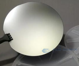
789nm AlGaInP / GaAs Laser Structure
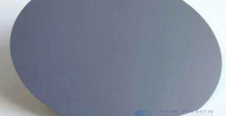
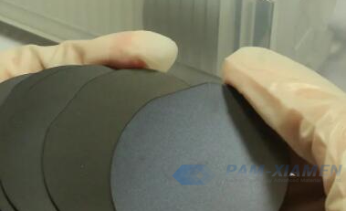
GaInAsP / GaInP / AlGaInP laser diode structure materials grown on GaAs substrate with a narrow waveguide is for fabricating laser diodes emitting wavelength at 789 nm. At present, the performance of infrared LD devices prepared by AlGaInP materials has surpassed other material systems. The semiconductor laser structure of AlGaInP / GaAs material system from Ganwafer is listed below for reference. Meanwhile, custom III-V epi structures for laser diode are acceptable.
1. AlGaInP Laser Structure on GaAs substrate
GANW200426-789nmLD
| Layer | d (nm) | Depth(nm) | Doping |
| n- GaAs Substrate (Si-doped) | – | – | n>1e18 |
| n- GaAs (Concentration) | – | – | – |
| n- GalnP (LM, Concentration) | – | – | – |
| n- ln0.50AlxGa0.5-xP (x: 0.00–>0.18; Concentration) |
– | – | – |
| n- ln0.50AlxGa0.5-xP (Concentration) | – | – | – |
| n- ln0.50AlxGa0.5-xP (x: 0.18->0.00; Concentration) |
– | – | ud |
| u – InGaP (LM, Concentratlon) | 150 | – | ud |
| u – lnGaAsP QW (CS,+1%) (λPL= 789 nm) |
– | – | ud |
| u- InGaP (LM, Concentration) | – | – | ud |
| u- ln0.50AlxGa0.5-xP (x: 0.00 –>0.18; Concentration) |
– | 2216 | ud |
| p- ln0.50Al0.18Ga0.32P (Concentration) | – | – | – |
| p- ln0.50Al0.18Ga0.32P (Concentration) | – | – | – |
| n- ln0.50AlxGa0.5-xP (x:o.18–>0.00; Concentration) |
– | – | – |
| p+- GalnP (LM, Concentration) | – | – | – |
| p++- GaAs – Cap | – | – | – |
2. Growth and Characteristics of AlGaInP for Laser Semiconductor
AlGaInP is a group III-V compound semiconductor material with the largest energy gap except for nitrides, and belongs to the metastable phase. Due to the inability to obtain its own substrate, GaAs should be selected as the substrate material. In order to meet the lattice matching with GaAs, the tunable range of AlGaInP material is very limited.
During the MOCVD growth process of AIGalnP laser diode structure, there are mainly the following issues worth noting:
1) The ordering problem of AlGaInP: The ordered structure of AlGaInP mainly affects the luminous efficiency, wavelength red shift and device stability of the material. In general, the generation of ordered structures should be avoided. The main measures are: choosing the proper growth temperature, II/V ratio and proper substrate orientation. Generally, an off-angle GaAs substrate is used for growing the AlGaInP quantum well laser structure. The off-angle substrate can also increase the p-type doping concentration in the confinement layer, thereby increasing the effective barrier of electrons in the active region, reducing the leakage of carriers, and improving the work performance at high temperature of the device.
2) The incorporation of oxygen can increase the deep energy level of the material, and the incorporation of oxygen in the active region increases the non-radiative recombination. The incorporation of oxygen in the confinement layer can reduce the hole concentration and make the preparation of P-type materials more difficult.
3) The matching problem between AIGalnP and GaAs is very important, but in the specific growth process, the thermal mismatch of different components should be considered to achieve one of matching and mismatching, and ensure the reliability and stability of materials and devices.
4) For laser technology, online detection plays an important role in improving the quality and repeatability of AlGaInP materials.
In addition, to improve the light-emitting properties of the AlGaInP material, new material structure is adopted. For example, quantum well strain structure, multiple quantum well structure and modulation doping structure gradient and moderate heterojunction structure, etc., the purpose is to improve the quantum efficiency and reduce self-absorption in the device of laser diode epitaxial structure.
For more information, please contact us email at sales@ganwafer.com and tech@ganwafer.com.

