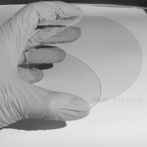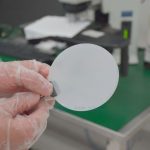
A Face Freestanding GaN Substrate


We offer a-plane Freestanding GaN Substrate including Si-doped, low doped and semi-insulating one. For Freestanding GaN, we have a history to control macro defects. Before 2000, we have dedicated research of GaN material. In 2007, we offer FS GaN on small quantity. In 2009, we offer FS GaN substrate on mass production, and we grade macro defects density: B grade: (5-10) cm-2 or A grade <5 cm-2. In 2011, we have a big improvement: for large size (2”), we can control them with macro defects (0-2) cm-2. The specification of a-plane (11-20) GaN substrate is as follows:
- Description
- Inquiry
Description
1. Si-doped A Face GaN Crystal Substrate
| Item | GANW-FS-GAN A-N |
| Dimension | 5 x 10 mm2 |
| Thickness | 350 ±25 µm 430±25 µm |
| Orientation | A plane (11-20) off angle toward M-axis 0 ±0.5° |
| A plane (11-20) off angle toward C-axis -1 ±0.2° | |
| Conduction Type | N-type |
| Resistivity (300K) | < 0.05 Ω·cm |
| TTV | ≤ 10 µm |
| BOW | -10 µm ≤ BOW ≤ 10 µm |
| Surface Roughness: | Front side: Ra<0.2nm, epi-ready; |
| Back side: Fine Ground or polished. | |
| Dislocation Density | From 1 x 10⁵ to 5 x 106 cm-2 |
| Macro Defect Density | 0 cm-2 |
| Useable Area | > 90% (edge exclusion) |
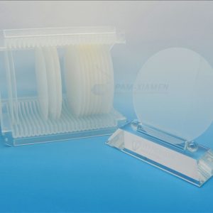
| Package | each in single wafer container, under nitrogen atmosphere, packed in class 100 clean room |
2. Low Doped Freestanding A Plane GaN Substrate
| Item | GANW-FS-GAN A-U |
| Dimension | 5 x 10 mm2 |
| Thickness | 350 ±25 µm 430±25 µm |
| Orientation | A plane (11-20) off angle toward M-axis 0 ±0.5° |
| A plane (11-20) off angle toward C-axis -1 ±0.2° | |
| Conduction Type | N-type |
| Resistivity (300K) | < 0.1 Ω·cm |
| TTV | ≤ 10 µm |
| BOW | -10 µm ≤ BOW ≤ 10 µm |
| Surface Roughness: | Front side: Ra<0.2nm, epi-ready; |
| Back side: Fine Ground or polished. | |
| Dislocation Density | From 1 x 10⁵ to 5 x 106 cm-2 |
| Macro Defect Density | 0 cm-2 |
| Useable Area | > 90% (edge exclusion) |
| Package | each in single wafer container, under nitrogen atmosphere, packed in class 100 clean room |
3. Free Standing Semi-insulating A-Plane GaN Substrate
| Item | GANW-FS-GAN A-SI |
| Dimension | 5 x 10 mm2 |
| Thickness | 350 ±25 µm 430±25 µm |
| Orientation | A plane (11-20) off angle toward M-axis 0 ±0.5° |
| A plane (11-20) off angle toward C-axis -1 ±0.2° | |
| Conduction Type | Semi-Insulating |
| Resistivity (300K) | > 10 6Ω·cm |
| TTV | ≤ 10 µm |
| BOW | -10 µm ≤ BOW ≤ 10 µm |
| Surface Roughness: | Front side: Ra<0.2nm, epi-ready; |
| Back side: Fine Ground or polished. | |
| Dislocation Density | From 1 x 10⁵ to 5 x 106 cm-2 |
| Macro Defect Density | 0 cm-2 |
| Useable Area | > 90% (edge exclusion) |
| Package | each in single wafer container, under nitrogen atmosphere, packed in class 100 clean room |
Remark:
The Chinese government has announced new limits on the exportation of Gallium materials (such as GaAs, GaN, Ga2O3, GaP, InGaAs, and GaSb) and Germanium materials used to make semiconductor chips. From August 1, 2023 on, exporting these materials is only allowed if we obtains a license from the Chinese Ministry of Commerce. Hope for your understanding!